Diligence and Technology Tame Static Charge
The principle is quite logical: By keeping all items at the same 0-V potential, there are no voltage differences to cause charge movement and possible damage to sensitive components. Although simple in theory, in practice, achieving an equipotential state can be daunting.
Each of the four ADNP actions addresses only a part of the overall static-control problem.
• Avoid—Remove unnecessary insulators such as Styrofoam cups from the work area. Bar nonessential people from entering a static-controlled area. If visitors really must enter, make sure they have put on ESD-safe smocks and footwear. Don’t let them touch anything.
• Dissipate—Charge will be generated within the work area, even if it’s just caused by the movement of the workers. Dissipative worksurfaces, floors, footwear, and wristbands ensure that most of the charge is returned safely to ground. ESD-safe storage bags are made from dissipative materials.
• Neutralize—Some insulating materials are unavoidable in the work area or may be part of the product being assembled. Ionizers provide a source of both positive and negative charges that neutralize static buildup. Ions can be produced electrically or by the decay of a radioactive substance.
• Protect—ESD-sensitive products are stored in bags having various properties. To gain the greatest degree of protection, a bag may have a conductive outer coating to shield its contents from the effects of an electrostatic field. The bag also will be made of or coated internally with a dissipative material to remove any charge that might otherwise build up on the product.
To be successful, an ESD control program must use all four procedures. In addition, ESD test equipment helps you understand the interaction among the different elements of such a program. In general, instruments measure charge or determine the properties of charge-control materials.
Static Control in Production
“We continue to educate users that a comprehensive program considers the net charge potential of many pieces of a program working together,” said Steve Heymann, CEO of Novx. “For instance, once an ESD-safe floor is in place, the customer needs to monitor the flooring in conjunction with the footwear to achieve the desired net result: minimization of the voltage on the operator.
“If the customer has determined that a dissipative floor is good by testing the resistance, that’s fine,” he explained. “But, if the customer’s operators don’t use good footwear in conjunction with that floor, the results will not be optimum. Even when both floor and footwear separately are good, we find that they may not work well together. Tribocharging can generate hundreds of volts when an operator walks around. Changing to a boot made of a different material can reduce the level to less than 10 V.”
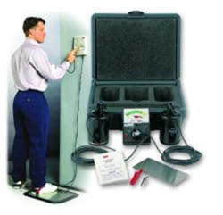
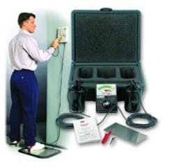
Dissipation and avoidance are the guiding principles in this example. The ESD Association’s ANSI/ESD S20.20-1999: Standard for the Development of an ESD Control Program specifies a procedure for determining floor resistance. A similar reference is found in ANSI ESD-S7.1-1994: Floor Materials—Resistive Characterization of Materials. To perform the test, two 5-lb probes, 2 ½” dia, are placed on the floor 3 ft apart, and the resistance between them is measured with a megohmeter.
A megohmeter measures from about 1 kW to teraohms (1012 W) and can provide the 100-V potential required for the floor resistance test. In contrast, an ohmmeter may operate at a 1.5-V level and measure from less than an ohm to a few megohms. Megohmeters aren’t limited to floors. Any flat surface including worksurfaces, packaging, and shelving can be tested in a similar manner. This general category is covered by ANSI ESD-S11.11-1993: Surface Resistance Measurement of Static Dissipative Planar Materials and ANSI/ESD S20.20.
Measuring the voltage on the operator’s shoe could be done with a noncontacting electrostatic field meter. Instruments from different manufacturers include a variety of features, but typical specifications are a 20-kV range at a distance of 1″ and a measurement hold capability.
Many of these meters use reflected light to determine that the 1″ distance has been reached. However, 1″ is not always the working distance as demonstrated by the 4″ measuring distance of the Tantec e-meter. It has a correspondingly greater 50-kV range. Accuracy can be 5% or better for this class of meter.
If you can sacrifice most of the portability afforded by the small, hand-held units, a meter that uses a separate detector may provide more measurement sensitivity and repeatability. A separate probe can have a much larger area than one built-in, and the charge induced on the sensing plate by the field you are trying to measure is proportional to the plate area.
Rotating vane sensors physically chop the electric field to produce an AC signal. This approach avoids errors due to the long but finite leakage time constant of the probe capacitance and amplifier input resistance. Rectification of the amplified signal in synchronism with the vane rotation generates the actual DC output.
Electrostatic fieldmeters are the basis of ionizer-balance measuring instruments. Ions from the ionizer are accumulated on a large sensing plate. If nearly equal numbers of positive and negative charges have been generated, the net voltage sensed is close to zero.
ESD Measurement
Charge is not necessarily static (pun intended). Charge moves from one region to another on a part, for example, and may move from one place to another quickly.
The problem of measuring ESD events was put into perspective by Mike Hopkins, director of sales and marketing at Thermo KeyTek. “The most difficult tasks associated with ESD measurements are the measurement and quantification of the ESD event itself. Measuring the static charge is relatively easy to do with inexpensive, commercially available instruments. But measurement of the discharge current and radiated fields associated with a discharge is extremely difficult to accomplish.
“Because ESD events contain energy at frequencies up to several gigahertz, high-bandwidth instrumentation is necessary to accurately measure the real discharge current,” he explained. “Some work has been done on the problem of radiated fields, but the ESD Association’s Working Group 14 committee is not yet in a position to publish methods for measuring these fields in a repeatable, quantitative way.”
ESD events are part of the environment in which many electronic products must operate. For example, you would become very upset if the cell phone in your pocket was damaged every time you received an ESD shock in dry weather. Products must withstand reasonable levels of ESD and so too must the individual electronic devices. One test instrument developed by Thermo KeyTek is used to qualify ESD protection on up to 768 individual semiconductor pins.
On the other hand, there is a static voltage limit below which an electronic assembly line should operate to ensure that no ESD-related damage will be caused. Jan Hoigaard, president of SpectraScan, was called in to investigate device failures that occurred on a line with only a few volts of potential difference—far too low a level to explain the problem.
“I suspected there were high-frequency transients riding on the electrical wiring. Such transients could contain frequency components exceeding 1 GHz and would not register on a multimeter because of its very low bandwidth,” he said. “I borrowed a 2-GHz scope and disconnected the electrical ground connection by floating the ground prong on the power plug. I then connected the scope’s ground to a true earth ground and used a 100:1 probe to measure the voltage on the AC supply line, neutral, and ground wires. I measured up to 1,200-V spikes on all three wires. The width of the transients was less than 1 µs, but it only takes a couple of nanoseconds to destroy an IC.
“It turned out that next door to the rework area where the failures were occurring was a large environmental testing area,” he continued. There, “50-hp electric motors driving shock and vibration machines were turning on and off continuously and corrupting the common electrical system. The device failure problem was solved by running the environmental lab and the rework area from separate electric circuits and installing transient filters on all the equipment in the testing lab.”
Decreasing ESD Tolerance
Very small-geometry semiconductors have a much lower tolerance to static charge than their 3-µm and larger ancestors. Mr. Hoigaard commented, “With today’s 0.1-µm geometries, the damage threshold often is just a few volts. From sheer necessity, ESD awareness is on the rise.”
To compound the problem, as semiconductor devices become smaller, their static charge becomes more difficult to measure. Dave Bermani, corporate marketing coordinator at Desco Charleswater, said, “Static charge can be accurately measured, providing the charged object is of a reasonable size. Often, the object in question is quite small, and normal charge measuring equipment is of no value.
“Static fieldmeters have what is known as an aspect ratio,” he explained. “This means that, at the normal 1″ measuring distance, the target object should be a minimum of 3″ square. This is an aspect ratio of three. Measuring charge on small items like ICs and magnetic recording heads requires very precise, specialized equipment.”
And, there are problems related to manufacturing methods. David E. Swenson, technical service specialist at 3M Electronic Handling and Protection Division, identified a shortcoming of present static measurement products: “The problem is associated with measuring the static charge accumulation on parts traveling through automated handling equipment. As more and more automated processes evolve, the ability to determine static charge and surface resistance and the ability of an ionizer to work in small areas are becoming critical. The ESD Association has a new standard relating to test methods for automated handlers, but freely admits that there is a shortage of instruments that can measure with fast enough response time to be useful.”
Mr. Heymann of Novx added some examples. “Laser diodes are susceptible to static levels under 10 V. There also is a correlation between static change and defect density within the semiconductor and flat panel display industries. Semiconductor Equipment and Materials International (SEMI) has created E78-0998: Electrostatic Compatibility Guide to Access and Control of ESD and ESA for Equipment. Other guidelines are being released that apply to a comprehensive static-control program within wafer fab and flat-panel manufacturing facilities. The International Disk Drive Equipment and Materials Association (IDEMA) is doing the same with documents such as ESD1-00: General Practices Standard for ESD Control Within the Disk Drive Industry,” he said.
Conclusion
In the questions we asked several ESD industry experts while gathering information for this article, we postulated that there was a relatively simple instrument for every need. While that’s true for measuring static charge on objects of reasonable size out in the open, it’s otherwise not. Actual dynamic ESD events are difficult to measure because of their speed, small-geometry parts tax instrument capabilities and have increased ESD sensitivity, and ionization is problematic within automatic handling equipment.
Most of the easy problems have been solved. Now it’s time to tackle the really difficult ones. Fortunately, change happens gradually. All modern ICs have not suddenly become supersensitive to ESD—a much smaller percentage of devices are supersensitive than not. Observing the time-tested ADNP principles hasn’t been made obsolete. In fact, a solid base upon which further static-control refinement can be built is more important now than ever before.
There still is room for improvement in the fundamentals of ESD control. That is evidenced by comments from one of the industry experts we contacted. “EOS/ESD management is isolated from the real soldiers out there in the trenches. When you are comfortable back at headquarters, everything appears to be in perfect order. Well, I’ve been to the trenches, and it ain’t!”
Return to EE Home Page
Published by EE-Evaluation Engineering
All contents © 2001 Nelson Publishing Inc.
No reprint, distribution, or reuse in any medium is permitted
without the express written consent of the publisher.
July 2001
About the Author
Comment About the Article
To join the conversation, and become an exclusive member of Electronic Design, create an account today!

Leaders relevant to this article: