Poor PCB track layout isn�t the only culprit causing radiated EMI. Here are some simple design techniques that can reduce EMI from high-speed ASICs.
Electromagnetic interference (EMI) is a latent problem the extent of which can only be determined after the entire system has been designed, built, and made operational. That�s when electromagnetic emissions measurements can be made to determine how much energy is radiated by the various active components in the system.
Besides the various regulatory limitations on far-field EMI, radiated energy can cause operational problems with any susceptible device located near the source of emissions. Since it�s well understood that high near-field emissions cause high far-field emissions�a problem for regulatory compliance�and can interfere with the operation of neighboring devices, system designers must spend more time looking at near-field sources of EMI.
EMI can be limited by attenuating the electromagnetic energy at the source of the emissions or ruining the efficiency of the radiating path. For applications where the active components are purchased off the shelf, a system designer can either contain the energy within a shield or degrade the radiating paths on the circuit board using careful layout techniques.
There is, however, only so much that can be done before cost and manufacturing concerns hamper further improvement. In those situations, additional reductions in EMI must be found by controlling the source of emissions at the component level. Integrated circuits operating at high frequencies can contribute significantly to overall radiated emissions.
For engineers designing high-speed ASICs, controlling EMI during the design stage is the most cost-effective approach. Some simple techniques such as the careful placement of what signals on which pins and the types of signaling protocols can lead to a considerable reduction of EMI.
The Basic EMI Problem
Radiated EMI is a complex relationship comprising an energy-emitting source, a radiating path, and a susceptible receiver. The active components, the circuit board layout, and the signals transferred among those components play a role in the strength of radiated EMI.
An electromagnetic wave consists of an electric field wave and a magnetic field wave traveling in the same direction but oriented perpendicular to each other (Figure 1). The dynamic electric field is generated by a periodically changing voltage potential similar to what would be found in a clock signal on a circuit-board trace. The corresponding magnetic field is created by a changing flow of the current.
Figure 1. Electromagnetic Wave
At points very close to the source of the radiation, the field that is produced will be mostly a function of the properties of the source. If the circuit contains high currents but low voltages, the resulting field will be magnetic. If the source has high voltage with little current, the resulting field is electric.
However, no wave is purely electric or magnetic. A conductor carrying a large current also produces a small voltage, and likewise an unterminated trace develops a small current in any parasitic capacitance.
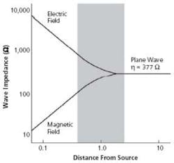
At points farther away from the source, both types of fields begin to attenuate, eventually becoming the same regardless of how the fields were produced.1 The ratio of the electric and magnetic fields becomes a constant called the free-space impedance (Figure 2).
Figure 2. Wave Impedance as a Function of Distance
Electromagnetic power emanating from a simple antenna can be estimated from:
The terms inside the parenthesis are constants such as h, the impedance of free space (377 W), and c, the speed of light.
Terms outside the parenthesis are variable and depend on the application. L is the length of the radiating path (the antenna), I is the current flowing in the radiating path, and f is the frequency. In most situations, the frequency is fixed by the application requirements. That leaves the current and length parameters as the focus of any EMI suppression efforts.
To relate these two terms to an ASIC, the current generally equates to the ASIC output driver current. The radiating path is formed by bond wires, the package lead frame, and the board traces.
A package lead frame consists of a regularly spaced arrangement of metal stampings that protrude from the nonconductive molding compound used to encapsulate the die. It also includes a stamped metal pedestal that forms a platform for attachment of the silicon die. Bond wires connect the pads around the periphery of the silicon die to the package leads.
Visualizing EMI
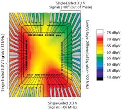
Figure 3 shows a high-speed mixed-signal ASIC that serves as a timing generator and contains two phase-locked loops with associated high-speed logic. The I/O pins are specified to drive a large capacitive load and have 30-mA single-ended output drivers.
Figure 3. Electric Field Radiation From Sample ASIC
On the left side of the ASIC, several pins provide 3.3-V PCI bus timing at a 33-MHz clock rate. Pins along the right side supply 3.3-V 66-MHz graphics timing information. Three channels of 100-MHz low-voltage differential signaling (LVDS) carry clock and data to and from an external microprocessor. Two single-ended 3.3-V timing outputs with signals 180� out of phase with respect to each other provide data timing for an external memory.
Three different output driver styles are used in this ASIC:
� Single-ended 30-mA outputs (VOH = 3.3 V) operating in phase at 33 MHz and 66 MHz.
� Single-ended 30-mA outputs (VOH = 3.3 V) operating 180� out of phase at 50 MHz.
� Low-voltage differential outputs (VOH = 0.75 V) operating at 100 MHz.
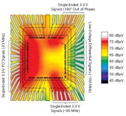
A visualization of actual near-field electromagnetic energy radiating from the example ASIC is shown in Figure 3 (electric field) and Figure 4 (magnetic field). Since the near-field emissions consist of separate electric and magnetic fields, both fields must be measured separately. Areas of red show high emissions; areas of green and blue indicate low-strength emissions.
These near-field emissions can be mapped to their associated signals and output pins. The single-ended PCI and graphics outputs contain strong electric and magnetic fields. The low-voltage differential outputs have very low electric and magnetic emissions despite operating at a frequency up to three times faster. And interestingly, the out-of-phase single-ended signals comprise a strong magnetic field but a relatively weak electric field.
Signal Loops
Equation 1 assumed energy was radiating from a simple dipole antenna. However, signal currents on a circuit board actually form a loop from the signal source to the signal receiver and back again.
Single-ended signals use a reference plane, usually the ground plane, as the return path for any current flowing in the radiating path. That reference plane often is shared with other signals, providing an opportunity for noise on one signal path to couple to other signal paths.
The power radiated from a loop antenna is shown in Equation 2. The length term takes into account the entire signal path, from emitter to receiver as well as the return path through the reference plane. In terms of EMI, a loop antenna in the form of a single-ended signal path makes an efficient radiating path:
(2)
Single-ended signals that are 180� out of phase with respect to each other benefit from some electric-field cancellation. Since the electric field is generated by voltage potentials, two equal but opposing voltage signals will cancel their respective electric fields. However, the single-ended return path still uses a reference plane to complete the loop, so signal currents do not cancel.2
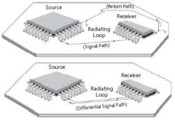
True differential signals follow an identical parallel path for the return loop, as shown in Figure 5. That results in a much smaller radiating loop length and allows for current cancellation. For those reasons, differential signals benefit from both electric- and magnetic-field cancellation.
Figure 5. Single-Ended (top) and Differential (bottom) Signal Loops
Since the magnetic field is generated by the flow of current, two equal currents flowing in opposite directions will cancel their respective magnetic fields. To maximize the benefit of differential clocking, board traces must be routed in parallel across the board to the receiver to keep the loop area small.3
Recommendations
Based on the near-field measurements and far-field power equations, some simple recommendations for reducing EMI can be developed:
� Single-ended clock and data I/O and their associated power and ground pins should go to the shortest center pins. That�s because the leads on the corners of the package are long relative to the leads at the center of the package. As a result, the radiating paths (bond wire plus lead frame) are the longest at the corner pins. The goal is to reduce the L in those power equations.
� Static digital pins can go to the longest corner pins since static fields do not cause EMI. However, this guideline does not necessarily apply to power and ground pins if those pins are associated with a set of single-ended rail-to-rail output drivers. That�s because the output drivers can inject a considerable amount of noise on the power planes.
� If rail-to-rail signals are required, use minimum-current output drivers where possible. The goal is to reduce the I in the power equations. For example, avoid the temptation to use a generic driver for a pad library since these pads may be over-designed for the application. Instead, consider a lower current driver or a slew-rate limited driver.
� Single-ended outputs operating at similar frequencies should be 180� out of phase with each other to obtain some level of field cancellation. Use true differential signals if enough pins are available.
� Keep the associated power and ground pins close to any single-ended signal pins to reduce the size of the signal loop.
� Using low-voltage signal protocols, like those shown in Figure 6, can dramatically reduce EMI simply because the signal amplitudes are smaller, requiring less current to charge parasitic and load capacitance. A combination of low-voltage protocols and differential signaling provides the optimal combination.
Figure 6. Representative VOH and VOL Levels
References
1. Capps, C., �Near Field or Far Field?� EDN, Aug. 16, 2001, pp. 95-102.
2. Fujimoto, K., et al, Small Antennas, Research Studies Press LTD, John Wiley & Sons, 1987.
3. Ingels, B.M. and Steyaert, M., �Design Strategies and Decoupling Techniques for Reducing the Effects of Electrical Interference on Mixed-Mode ICs,� IEEE Journal of Solid State Circuits, Vol. 32, July 1997, pp. 1136-1141.
Johnson, H. and Graham, M., High-Speed Digital Design: A Handbook of Black Magic, Prentice Hall, 1993.
Hall, S., et al, High-Speed Digital System Design: A Handbook of Interconnect Theory and Design Practices, John Wiley & Sons, 2000.
About the Author
Carl Falcon is in strategic marketing at AMI Semiconductor. He holds a B.S.E.E. and an M.S.E.E. from Drexel University and an M.B.A. from St. Joseph�s University. He joined AMI in 1997 as a design manager. Mr. Falcon is a senior member of the IEEE and has authored several articles on mixed-signal CMOS ASIC design. AMI Semiconductor, 2300 Buckskin Rd., Pocatello, ID 83201, 208-233-4690, e-mail: [email protected]
June 2004


