The variety of different test methodologies combined with today�s mixture of memory devices creates a complex test profile.
The manufacturing test floor hums with activity; a range of memory devices is being tested on a variety of testers. There may be different combinations of DRAM, SRAM, flash, embedded, and stacked memories all requiring test on a single manufacturing floor. More than ever, memory manufacturers are facing product-mix issues among the various memory technologies.
In the past, a test floor was populated by a single type of memory device, such as DRAM or flash, and a tester was chosen with this device in mind. But now, the memory market is in transition. No longer are manufacturers dedicated to one memory type, and no longer do they have the luxury of using test platforms tailored to a specific target device. To remain competitive, they have no alternative but to diversify their product mix.
Memory manufacturers also face another challenge: variety within a single product type. As device densities and pin-counts have increased, manufacturers have created alternate test methodologies that enable a device to be tested with a reduced set of pins at different steps of the process. However, since these methodologies are new and must be considered in the design of the product, they may not be uniformly applied throughout the product family. Newer devices may be designed with the test methodologies while older ones are not.
Additionally, different test methodologies may be used at different times during the life cycle of the device. This results in a mix of high and low pin-count devices, both of which need to be tested cost effectively, adding complexity to the product-mix challenge. Wafer sort poses particular problems since the test needs of memory products are more diverse than at final test.
Consequently, the question is how to accommodate not only different memory types at wafer sort, but also different test methodologies. The answer is not multiple test platforms, one dedicated for each device type, because that introduces too much complexity in many of the manufacturing processes: operator training, maintenance and support, test development, and product support.
Also, a tester dedicated to a specific product may have a short life if that product has a short lifetime. Instead, a flexible system that can provide high throughput and parallelism while dynamically changing to accommodate different pin and parallelism requirements may be a better way of meeting the challenges of memory mix test.
Memory Mix Market
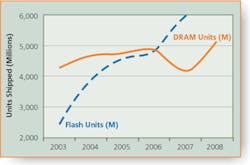
The semiconductor memory market has experienced great fluctuation over the past several years. Market drivers such as the PC, once the primary driver for memory devices, are being augmented by communications, consumer, and computing applications expanding from stationary to wireless and mobile use. Flash memory, well suited for mobile devices, is experiencing an explosive period of growth (Figure 1).
Recognizing the growth of the nonvolatile memory market, DRAM manufacturers are crossing over into flash memory. In the past, the different memory manufacturers clearly were defined by memory type: Intel was the leader in flash memory and Samsung the leader in DRAM memory.
Now Samsung as well as Micron, Hynix, and Infineon, all DRAM suppliers, are expanding into flash memory or rapidly expanding their existing flash memory lines. Pure NOR flash suppliers such as STMicro and Spansion, an AMD�Fujitsu joint venture, are adding NAND flash to their product mix. These crossover manufacturers, as well as subcontractors, need a test system that can accommodate a varied product mix.
Memory Test Requirements
At wafer sort, DRAM devices exhibit typical pin-counts of less than 60 pins and are tested at frequencies up to 200 MHz. For DRAM, a stimulus is applied to the memory cell, the memory cell is read and compared to expected data, and then fail flags are set accordingly.
DRAM test requires an algorithmic pattern generator (APG) rich with features to write complex patterns typically found in DRAM test. Because DRAM is a commodity product vulnerable to market fluctuations, minimizing the cost of test is critical.
One way DRAM manufacturers try to lower the cost of test is through high parallelism. Another way reduces the number of pins required for test by using compression techniques.
SRAM devices target different applications than DRAM, and performance requirements also may differ. Despite these differences, many of the test techniques used for DRAM are applicable to SRAM.
Flash testing differs from DRAM testing in significant ways. For flash test, the exact value of the stimulus to apply to the memory cell is not known and must be determined through an iterative process. It is uncertain how long it will take to complete a test step once it�s begun.
As a result, the test time for each cell is not exactly the same as it is for DRAM. Flash, particularly NOR flash, requires an APG that provides independent sequencing on a per-device under test (DUT) basis. Like DRAM producers, flash manufacturers try to reduce the cost of test through high parallelism and different test methodologies at wafer sort.
Emerging Test Methodologies at Wafer Sort
As the cost of test continues to rise, different methodologies that reduce the number of pins required to test a device are being implemented. These methodologies share the benefits of smaller pin-counts, reduced tester resources, and higher throughput but have an impact on device design.
Some DRAM manufacturers use compression techniques to reduce I/O pins from a typical eight or 16 channels down to four. Fewer tester channels are needed with the compression scheme; however, a longer, more complicated test program is required.
Flash devices, both NOR and NAND, use full pin-count (FPC) and reduced pin-count (RPC) test methodologies. With an FPC strategy, all device pins (generally <52) are accessible, providing maximum flexibility for test generation. Bitmapping and many redundancy schemes are available, with redundancy analysis performed by the ATE.
The FPC test methodology provides the most extensive, flexible coverage since all user-mode functions and data-sheet parameters can be tested. However, this methodology has the most intensive capital cost and is required for known-good die and final test.
RPC test methodologies are very similar to the FPC technique but apply to fewer pins. The DUT interface is reduced to about 16 pins or less, depending on the bus width of the multiplexed address and data pins. Some built-in self-test (BIST) capability may be needed to handle algorithmic operations such as automatic address and data generation. RPC results in higher throughput, but some tests, such as at-speed tests, cannot be covered 100%.
BIST methodologies are more minimized than other techniques and can be applied to DRAM, SRAM, or flash. BIST is more appropriate once a part is mature since access to the part can be very limited.
The DUT interface is a serial interface and requires eight or fewer pins, and the device can be completely controlled by the BIST controller including all program/erase algorithms. The BIST controller executes all trimming and redundancy analysis with a simple column or block redundancy.
The ATE is only required to perform DC tests, provide a voltage/current reference, sequence through BIST functions, and process the pass/fail information. BIST reduces the need for high-performance ATE, but this comes at the cost of die-size penalty.
At this point, there is no one right test methodology. Since some of these techniques are emerging, time is required to develop and deploy each methodology. Even once the methodologies are mature, they will correspond to different times in the life cycle of the device.
Full pin-count methodologies will be used on first silicon and for charac-terization; reduced schemes such as I/O compression, RPC, or BIST will be used once the part is mature. Because of the unique test requirements at different points along the device life cycle, there always will be a mixture of test methodologies on the test floor.
The variety of test methodologies�I/O compression, FPC, RPC, and BIST�combined with the mixture of memory devices is creating a complex test profile. In this environment, an ideal test system would be able to switch from one memory technology to another while maintaining high throughput, high parallelism, and the capability to adjust to different pin-counts and parallelisms.
High Throughput
In a memory mix environment, it is important to have an ATE architecture that can maximize throughput for all the memory types. Two typical architectures used to test memory devices are shared resource and tester-per-site.
With a shared-resource architecture, it is necessary for each DUT to wait for serial resources when needed. Contrast that to a tester-per-site architecture in which each DUT receives its own dedicated set of test resources�APG, buffer memory, error-catch RAM, vector memory, and power supplies. No critical resources are shared. This distinction is important for serial tests that require unique data for each DUT, such as electrical repair and parametric tests, as well as flash programming.
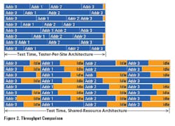
The architecture type has a direct influence on test time. With the shared resource architecture, the serial tests on one site must be completed before testing can begin at the next site since only one set of resources is available for the whole system. As a result, the nonoperating DUTs remain idle until the resources are available to test them. In this case, the total serial test time is the sum of the test times of all the individual DUTs.
With a tester-per-site architecture, each DUT can be tested independently in parallel since there is one complete set of test resources behind each site. The DUTs do not have to wait for resources, and the total test time is only as long as the slowest DUT (Figure 2). The tester-per-site architecture results in a much higher throughput for devices that are asynchronous in nature, such as flash memory.
DRAM and SRAM typically are tested with shared-resource ATE architectures because the devices have a predictable, deterministic behavior, and sequencer control can be the same for all DUTs. Sharing the controller, buffer memory, and APG resources reduces tester cost.
On the other hand, testing NOR flash requires more than just the functionality of DRAM and SRAM test. In particular, NOR flash is difficult to test without allowing for independent sequencing within the APG on a per-DUT basis.
Without per-DUT sequencing, test times increase by 15% to 25% per each additional device tested due to serialization of shared tester resources. The additional test time required for each additional DUT is known as test-time overhead (TTO).
For this reason, NOR flash historically has been tested on an ATE tester-per-site architecture. This architecture also provides a controller per DUT so that the test programs and not just the pattern-generated code can run independently.
Independent computational power per DUT allows the test flow and test patterns to be modified dynamically per DUT as pass/fail information and array behavior, such as program or erase time, are accumulated. Program development also is greatly simplified since no attention needs to be paid to managing multiple DUTs.
NAND flash requires the same basic requirements as NOR flash, DRAM, and SRAM. However, in the case of NAND flash, the choice between tester-per-site or shared resource architectures is not so clear. The decision depends on the test methodology, test modes, and other business factors. Issues such as product mix, NAND/NOR/DRAM, NAND/DRAM, or NAND/NOR often influence the decision.
Consequently, since the tester-per-site architecture results in a much higher throughput for devices that are asynchronous in nature, such as NOR flash and certain NAND flash memory, it is necessary to have this architecture when testing a mix of memory products that includes flash. The most flexible tester-per-site architectures offer greater than 128 sites per system with at least 32 I/O channels per site. This translates into the capability to test more than 256 DUTs with more than 4,000 I/O pins per test system.
High Parallelism
Different memory types require high parallelism that, in turn, is being driven by expanded die size and large-area wafer probing. At wafer sort, dual test heads with high pin-counts achieve high parallelism for DRAM, up to �128.
For flash memories, a tester-per-site architecture paired with high pin-counts is necessary to provide similar parallelism rates. However, as tester pin-counts increase, significant connection-count problems arise between the ATE pin electronics and the probe cards or load boards. This is an industry-wide problem.
Part of the problem is the large number of pins needed in the ATE interface. Even though a user only may access I/O channels, drive channels, and utility channels, the tester interface needs more than twice as many pins since each signal pin often is accompanied by at least one or two grounds to maintain the required 50-? impedance. For example, a highly parallel system of more than 128 sites provides more than 4,000 channels. However, the DUT interface for that same system is composed of more than 11,000 pins.
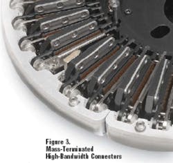
With the traditional pogo-pin interface, the amount of force required to seat an 11,000-pin interface to a probe card would be around 700 lb. This high seating force would result in planarity and consistency problems, casting doubt on the reliability of the pogo-pin solution. As the tester interface exceeds 11,000 pins, it is imperative that a reliable DUT interface be provided.
Flexible Configuration
The combination of memory products�DRAM, SRAM, and flash�and their associated test methodologies�I/O compression, FPC, RPC, or BIST�results in a variety of different parallelisms and pin-counts. Wafer-sort parallelisms can range anywhere from �128 to �36 and pin-counts from 60 to four.
In this situation, configurability of tester resources is very important. Having all I/O pins vs. dedicated drive-only and I/O pins helps accommodate a wider variety of device types. In addition, when using tester-per-site architecture, the capability to adjust the number of pins associated with each APG helps optimize parallelism without wasting tester channels.
Since memory devices present such a varied combination of pin-counts and parallelisms, it is imperative that a tester have the capability to adapt to this variation. When NOR flash and certain NAND flash memories are part of the product mix, a flexible configuration that enables the APG to adjust to different DUT pin requirements is essential for optimizing parallelism.
Summary
The mix of DRAM, SRAM, and flash memory products combined with a mix of I/O compression, FPC, RPC, and BIST test methodologies presents a complex test profile. At wafer sort, it is critical that the memory test system supports a range of pin-counts from under 10 to more than 60 and a range of parallelism needs from �36 to �128. The basic test functions of program, erase, datalog, redundancy analysis and repair, and trim and margin measurements are required. Also, the test architecture must be able to handle DRAM and SRAM testing and flash testing equally well.
To meet the issues facing memory manufacturers today, testers at wafer sort require a broad range of capability including:
-
Tester-per-site architecture with dedicated resources for each DUT to maximize throughput.
-
High pin-counts and a mass-terminated high-bandwidth DUT interface that provide the reliability high pin-counts and high parallelism require.
-
A flexible configuration that dynamically adjusts the number of pins associated with each APG to efficiently use tester channels and optimize parallelism.
About the Author
Sam Wong is an applications engineer for the Memory Test Division at Agilent Technologies. Prior to joining HP/Agilent in 1995, Mr. Wong worked at several semiconductor companies in the area of memory and logic test development for more than 10 years. He holds a B.S.E.E. and an M.S.E.E. from Santa Clara University. Agilent Technologies, 5301 Stevens Creek Blvd., Santa Clara, CA 95051-7201, 408-553-7004, e-mail: [email protected]
August 2004
About the Author
Voice Your Opinion!
To join the conversation, and become an exclusive member of Electronic Design, create an account today!

Leaders relevant to this article:


