Improving the Structural Stability Of Probe Cards

Simple mechanical changes can significantly improve probe card performance.
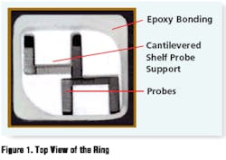
Epoxy-ring probe cards with 2,000 or more probes are economical solutions to multi-DUT parallel test. The key to repeatable high performance has been refining the so-called ceramic-shelf design.
As in conventional epoxy-ring construction, one or more layers of cantilever needle probes are attached by epoxy to a ceramic base. Shelf probes feature a ceramic base with strategically placed slots along three sides of a shelf. Groups of probes are attached to the ceramic base and the shelf to form a four-sided contact pattern.
This construction provides uniform probe mounting. All the probes in a group have the same cantilever length and, with precise manufacturing, will exhibit nearly perfect planarity and uniform contact force. Because only a few different tip lengths are required, the behavior of all the groups of probes can be controlled within a tight tolerance.
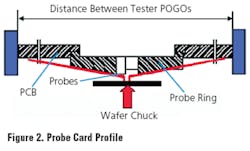
The technology used in multidie cards is similar to that found in smaller cantilever needle probe cards, but when the large number of probes touch down, high forces cause structural deflection. Only the probes are intended to bend, but the ceramic shelf and the thick FR4 PCB probe card also deflect under load. In Figure 2, the original design shows the through opening in the support PCB and the ceramic base glued into a rebate around the lower part of the opening.
Because stresses associated with the ceramic-shelf deflection could produce cracks and sudden mechanical failure, a detailed understanding of the mechanical system was undertaken.
Measuring What Is
Touchdown of a wafer on the dual-die shelf probe card is designed to produce 2.5-mil overtravel (OT). This corresponds to a nominal 4.375g at the specified 1.75g �20% per mil OT. Taking into account the �20% tolerance, the actual force could be as low as 1.4g per mil or 3.5g.
Deflection of the probe card PCB reduces this value even further because it decreases the effective OT. Allowing �0.00025″ for planarity tolerance and assuming 0.0005″ for probe card deflection, the maximum OT could be only 0.00175″ for some probes, resulting in 2.45g and, as a result, a high probe contact resistance.
A digital dial indicator with low contact pressure was used to measure the deflection of the probe card under load. Measurements were taken at the tip of one of the ceramic shelves, at the shelf base, in the corner of a shelf, and on the top of the PCB. To improve the statistical confidence of the measurements, 100 sets were taken: a touchdown was performed, measurements were made, and the load was removed 100 times.
As might be expected, the deflection at the cantilevered shelf tip was greatest, varying from 0.00060″ to 0.00095″ over the course of the 100 touchdown cycles. The behavior of the corner and the behavior of the base of a shelf were similar, varying from 0.00045″ to 0.00065″. The PCB deflected from 0.00025″ to 0.00040″. The mean values of these measurements were 0.00072″, 0.00057″, and 0.00034″, respectively.
When theoretically considering the various effects that could alter the probe force from its design value, more than a 40% decrease resulted if only a 0.0005″ deflection were assumed together with the 0.00025″ planarity tolerance. This small amount of unintended deflection is important, and the actual measured deflection is even larger.
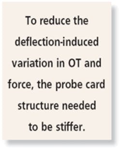
To reduce the deflection-induced variation in OT and force, the probe card structure needed to be stiffer. Before investigating possible solutions, a finite element (FE) model of the unmodified probe card was developed. Previous attempts to apply analytical solutions to the assembly had only limited success.
Modeling the Probe Card
The basic equation for the deflection of a clamped circular plate under a uniform load applied over a small circular area is straightforward but doesn�t exactly fit the real situation. The probe card doesn�t have the assumed uniform thickness, nor is it made of a homogeneous, isotropic material. In addition, the analysis needed to provide specific information about stress concentrations within the complex, machined ceramic ring. An analytical solution wasn�t appropriate for this level of detail.
A full-scale FE model was necessary. This model accounted for as many design details as practical, including separate material properties for the ceramic, copper, and FR4 elements of the probe card assembly. The real design�s dimensions were used and a touchdown simulated. Simulation results for the overall deflection correlated well to the experimental measurements.
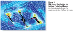
Figure 3 shows a color-graded stress distribution map of the ceramic ring area. The maximum calculated stress was 2,600 psi, which was very high. Although the flexural strength of the ceramic is about 15,000 psi, material defects or propagation of a microcrack could cause a brittle fracture. Stiffening the assembly to reduce deflection also should lower the peak stress level.
Recommendations
Modifications to the ceramic ring didn�t seem warranted. Manufacturing steps associated with the ring were carefully developed and painstakingly proven. To make alterations in this part of the assembly was the least desirable approach. Instead, efforts concentrated on the mounting of the ring to the PCB and adding a separate stiffener.
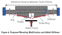
In the unmodified probe card, the ceramic ring was glued into a rebate cut in the PCB�s round central opening. The first step in creating the new, strengthened assembly was to eliminate the PCB cutout and replace it with a shallow depression into which the ceramic ring could fit. In addition, a ceramic stiffener was designed to cover as much of the PCB top surface as possible (Figure 4).
The FE model was updated to include both changes, and deflection and stress simulations were run again. This time, the maximum ring deflection was reduced to only 0.00015″ at 2.5-mil OT. The entire structure had become much more rigid and uniform without the central cutout. Because of this, the ring deflection across the entire ring area was very uniform, exhibiting a standard deviation of only 0.00003″. Most importantly, the simulated changes reduced the maximum stress to 835 psi�a 67% reduction.
Building a probe card that incorporated the recommended modifications would determine whether the changes really worked as expected. Dial-indicator measurements were made on top of the ceramic stiffener near its center and at its edge farthest from the center. The PCB deflection near the stiffener edge also was measured.
Results showed significant deflection reductions compared with the original design. Although it was not possible to directly compare the ceramic-shelf deflections after the central cutout had been removed, the PCB deflection reduced from 0.00034″ to 0.00016″. It�s reasonable to assume that the 0.00018″ improvement directly affects the original ceramic-shelf deflections.
It�s interesting to note the very small difference between readings at the center of the ceramic stiffener and at its edge. Because there is such a small change, the ceramic element essentially is not bending. This means that the difference between the displacements at the stiffener edge and on the PCB must be accounted for by elasticity in the epoxy joint or in locally concentrated bending of the PCB at the PCB/ceramic stiffener joint. In any case, the deflection being considered is only 0.0001″.
Conclusions
The FE modeling of the overall probe card assembly provided simulation results that correlated well with experimental test data. As a result, FEA is a reasonably accurate assessment tool to help understand the behavior of complex probe cards.
In addition, a real probe card design was improved by constraining unintended deflection of the support PCB. More uniform probe force and OT resulted from changes to the interface between the PCB and the ceramic ring. An additional stiffener also contributed to the improvement.
Reference
This article was developed from a presentation made at the 2004 Southwest Test Conference. The paper, entitled �Structural Stability of Shelf Probe Cards,� is available in its entirety at www.swtest.org/swtw_library/2004proc/PDF/S05_01_Dabrowiecki.pdf.
About the Author
Krzysztof Dabrowiecki is R&D director at Probe 2000. Previously, he was a product development manager at PTC and K&S. Mr. Dabrowiecki, a member of ASME, earned bachelor�s and master�s degrees in mechanical engineering at the Technical University of Gdansk, Poland. Probe 2000, 580 Charcot Ave., San Jose, CA 95131, 408-577-0970, e-mail: [email protected]
October 2004
About the Author
Comment About the Article
To join the conversation, and become an exclusive member of Electronic Design, create an account today!

Leaders relevant to this article: