EVM testing could be the answer to determining end-to-end performance while greatly reducing test time.
As increased levels of integration become more commonplace in wireless designs, new approaches must be developed to address the associated test challenges. Today, two-chip solutions play a dominant role in wireless local area networking (WLAN) 802.11 architectures.
Typically, the interface between these devices, the radio and the baseband processor, is an analog in-phase (I) and quadrature (Q) link. Traditional measurements to quantify the performance of this link include analyzing filter responses, magnitude and phase imbalances, and other parametric measurements.
As this signal interface moves to a digital link or disappears altogether as these devices are integrated, traditional metrics no longer apply. Error vector magnitude (EVM) testing in the ATE environment offers a new way to characterize devices at the system level to provide more meaningful test data while helping to drive down test costs.
While EVM measurements have existed in the design environment for a number of years, the test time typically was on the order of seconds, which is impractical in a high-volume, price-competitive market like WLAN semiconductors. Recent advances in ATE solutions, including approaches such as parallel wideband receivers, and distributed DSP processing allow these measurements to be made cost-effectively in production.
WLAN Transceiver Cost Pressures
The WLAN market is growing rapidly to meet consumer demands for high-speed mobile data transmission. In 2003, WLAN 802.11 chipset revenue grew by 74% to $760 million from $436 million in 2002. Unfortunately for equipment and device providers, shipments increased at an even larger rate.
This great disparity between shipment growth and revenue growth is placing enormous cost pressures on the WLAN semiconductor industry. As a result, new approaches must be taken to preserve the extremely thin profit margins that semiconductors typically operate on. While much has been done in the process technology arena using 0.18-�m CMOS processes even for RF transceivers, test methodology often is neglected as an area for improvement.
Today, many transceiver test philosophies remain rooted in the past. Too often, test and product engineers specify a litany of tests based on low-level characterization approaches. These tests include various measurements such as I and Q magnitude and phase, DC offset, and phase noise. While advances in ATE hardware can help speed these tests along or reduce the cost of the equipment, a fresh look at device test is needed to meet the step-function cost reductions needed.
WLAN Transceiver Architecture
To meet aggressive cost targets and compact packaging requirements, virtually all WLAN 802.11 system implementations have moved to a two-chip architecture. Typically, this consists of an RF-to-baseband transceiver, which is primarily RF and analog, and a baseband interface chip that basically is digital and mixed signal.
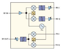
Focusing on RF test methodology, a typical zero intermediate frequency (ZIF) transceiver is shown in Figure 1. While various implementations have intricate details to deal with blocking and DC offset issues, the basic topology remains the same.
ZIF Architecture Performance Challenges
In moving from a super-heterodyne to a ZIF implementation, various performance issues become significant:
� As the communications signal is being down-converted to DC or very near DC, flicker noise (1/f noise) can become a problem. The point at which the thermal noise floor of the device and the flicker noise coincide is called the 1/f corner frequency. 1
For many CMOS processes, this may be on the order of a few kilohertz. So if the modulation has signal energy near DC, then the increased overall noise floor will be higher, resulting in degraded noise-figure performance. This will limit the range and data rate that can be obtained in a WLAN system.
� Since the local oscillator (LO) typically is built into the transceiver, it can leak into the RF input chain, either through the low noise amplifier (LNA) or other coupling, and mix with a phase-shifted copy of the LO signal coupled through another path in the circuit. The result is a DC component at the output of either the I or Q channel.
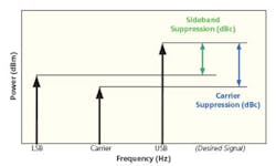
� Gain and phase imbalance between the I and Q channels can cause poor carrier and sideband suppression in the transmitter section. Typically, the baseband section of the device can have gains of 40 to 80 dB. At such levels, it can become difficult to precisely control the gain and phase matching between channels. Figure 2 illustrates carrier and upper and lower sideband suppression in a transmitted spectrum.
Verifying ZIF Device Performance
Given the numerous design challenges in implementing a ZIF transceiver, test becomes especially critical to ensuring good system performance. Due to the process-pushing nature of these circuit designs, simply guaranteeing specifications by design usually is not feasible. For this reason, these devices need to be tested.
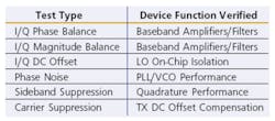
The traditional test approaches to ZIF designs consist of numerous continuous wave (CW) parametric tests that ensure device functionality by functional block as summarized in Table 1. This approach has advantages and disadvantages. For a designer, these low-level tests can provide valuable feedback about the individual functional blocks of the device and how they are performing.
For the system engineer, these tests may not be as meaningful. For example, if the I/Q phase balance is off by 2� but the phase noise is better than the specification by 5 dBc/Hz, there is a question whether the system can operate as desired. This example indicates how predicting system performance from a myriad of functional tests is difficult, if not impossible.
The functional block test model certainly has the potential to make system performance specification difficult. Even more onerous is its impact on the cost-of-test for semiconductor devices with very tight profit margins. A new test methodology is required to ensure overall system performance while maintaining the economic viability of producing devices for the WLAN market.
System-Level Test and Performance Verification
Specifying a good device test regimen is as much about philosophy as it is about technology. The test engineer and the product engineer must clearly agree on the goals of the test strategy to be used. Very often, these goals may change depending on what stage the product is in relative to its life cycle.
For example, when the first devices are being produced, a functional block test strategy may be very useful in determining precisely how the LNAs or the
I/Q demodulator circuits are functioning. However, as the silicon is proved out and cost concerns become more crucial in the high-volume phase of the product, a re-evaluation of test strategy may be required.
While for some devices this simply may mean turning certain tests off, that typically will not be a safe approach for advanced transceivers. The test organization needs to look at system-level tests to ensure device performance while minimizing costs. A cost-effective test strategy for wireless devices should guarantee specified system-level performance while also ensuring the device in question does not adversely affect other users of the radio spectrum. With these two goals in mind, a choice of test strategy becomes clear.
EVM is one such test that holds enormous potential to guarantee system-level performance. It is effective in determining end-to-end performance while allowing vast reductions in test time.
In a digital transmission system, data is encoded as symbols. A symbol represents the number of encoded data bits that varies depending on the standard. For the 802.11a standard, up to 64-state quadrature amplitude modulation (64-QAM) is used to achieve the highest data rate of 54 Mb/s.
A constellation diagram depicts where the symbol points must lie. With higher-order QAM systems, there is less room for error. Deviation in phase and amplitude can cause adjacent symbols to be misinterpreted by the receiver and cause a transmission error.
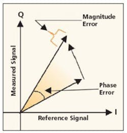
EVM provides a single number metric, usually expressed as a percentage (0% being ideal) that corresponds to the overall system performance in terms of a constellation diagram.
As shown in Figure 3, EVM relates the error vector, both magnitude and phase, to the reference vector. The result is expressed as a percentage relative to the reference vector. From a system point of view, EVM gives a single value that ensures system performance to a specified level. It contains all the needed information other than, perhaps, power consumption and thermal requirements.
Constellation Diagrams for Device Analysis
By itself, EVM cannot provide much useful information about why a particular device is failing. However, the constellation diagram, which must be analyzed to get the EVM value, offers a wealth of information. Since all errors in the device combine in some fashion to create a nonideal constellation diagram, analysis of a constellation diagram allows insight into the device�s performance. Figure 4 illustrates various device maladies that may be observed from a constellation diagram.
In Figure 4, three error cases are shown. In the first case, the relative gain between the I and Q channels is not equal so the constellation appears stretched in the I direction. This would imply that either the I channel has too much gain or that the Q channel has too little.
In the second case, a circular smearing is evident, causing the constellation to appear as though it is rotating in time. This type of presentation is particularly useful because phase-noise testing can be quite time-consuming, ranging from 100 ms for a particular frequency to many hundreds of milliseconds depending on the phase-noise performance to be quantified.
Quadrature error is visible in the third case. In this instance, the relative phase between the I and Q channels is not 90� so the constellation takes on a rhombus appearance.
As is evident from Figure 4, constellation diagrams and the use of EVM calculations can replace numerous functional block tests and still provide good diagnostic information for the resolution of device maladies. In fact, using an EVM approach with constellation diagrams can eliminate all the tests listed in Table 1. This provides a powerful tool to quickly and accurately characterize system and device performance.
Conclusion
ZIF devices used in nearly every cellular and WLAN radio represent a technological challenge to the wireless semiconductor industry. The combination of high device performance requirements with a very low selling price conspires to make test costs even more of a concern.
Taking a fresh look at test methodology can find innovative means to meet this challenge. This requires the cooperation of the various entities within semiconductor companies and use of metrology expertise provided by the ATE industry. Innovative test approaches combined with ATE hardware tailored to these new test requirements can deliver the step-function cost-of-test reduction necessary to make wireless semiconductor manufacturing a profitable endeavor.
Reference
1. Loke, F. A., �Direct Conversion Radio for Digital Mobile Phones�Design Issues, Status, Trends,� IEEE Transactions on Microwave Theory and Techniques, November 2002, Vol. 50, pp. 2422-2435.
About the Author
John Lukez is the product marketing director for the ASL RF product line at Credence Systems. Mr. Lukez has spent his career working with wireless test solutions that range from R&D test methodology to ATE solutions. He holds a B.S.E.C.E. from Ohio State University. Credence Systems, 1421 California Circle, Milpitas, CA 95035, 408-635-4800, e-mail: [email protected]
January 2005
About the Author
Voice Your Opinion!
To join the conversation, and become an exclusive member of Electronic Design, create an account today!

Leaders relevant to this article:


