New Architecture Enhances Memory Test and Repair
Generic test and repair approaches to embedded memory have hit their limit.
Smaller feature sizes, such as 130 nm and 90 nm, have made it possible to embed multiple megabits of memory into a single chip. However, these newer technology nodes have contributed to complex design rules and expensive fab and mask costs.
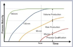
The newer technologies also are slow to mature, leading to high defect densities and low yields (Figure 1). The end results are escalating product development and manufacturing costs along with fierce competition that has tightened product and market windows, making it necessary to ramp up to volume quickly. Managing yield can mean the difference between profits and losses in these market conditions.
Densely packing the memory bits makes them prone to manufacturing failures. A semiconductor with equal areas of memory and logic is likely to fail due to manufacturing defects in memory twice as many times as it will due to defects in logic. Since the IC has both memory and logic, it is the memory that determines the overall yield of the system on a chip (SOC).
Repaired memories lead to failed chips being recovered, with overall yield improvements and substantial savings in manufacturing costs. But it is not enough to have repairable memories. It also is imperative to have the correct solution for the on-chip test and repair intellectual property (IP) to ensure the best repair efficiency.
Evolution of Embedded Memory Test and Repair
Prior to the advent of the 180-nm process technology, designs were characterized by few memories totaling less than a megabit, and chip area was dominated by logic. Consequently, overall yield was determined by the logic yield, and memory repair was only needed early in the process life cycle.
A typical solution was to have memories with spare elements (redundancy) from one vendor and an on-chip test solution from a third-party EDA company referred to as built-in self-test (BIST). In such solutions, external diagnosis and redundancy analysis were sufficient to achieve satisfactory yields.
The 180-nm designs tended to have a few large blocks of memory totaling a couple of megabits. Previous techniques became inadequate for embedded memory test and repair. An unintegrated approach of sourcing embedded memory IP from one vendor and BIST from another vendor led to test escapes and improved, but suboptimal, yield. A difference of 5% in yield can mean as much as $10 in extra cost per chip for a large IC, translating into tens of millions of dollars of added cost for applications running in high volume.
To address this challenge, an integrated solution for embedded memory test and repair is needed in conjunction with all the functions of the system. Such a system then can appropriately detect faults and repair them to the maximum extent possible while minimizing overhead due to area and performance.
The 130-nm process node brought about an explosion of process options to suit the appetites of an increasingly segmented semiconductor industry: multiple megabits of embedded memory and a mixture of different memory architectures in the same design to optimize power and save area plus a mix of repairable and nonrepairable memories of small, medium, and large sizes.
An embedded memory test and repair solution must include ways to test and repair multiple memory architectures, types, and sizes, and there is a need for differing memory redundancy schemes. The type of memory redundancy depends on the types of defects observed. Row redundancy has to be introduced to recover memory failures resulting from a single defect affecting adjacent memory locations. Differing redundancy schemes and fault types call for differing test and repair algorithms.
One generic test and repair engine is inadequate to address the different memory faults affecting different memory types and architectures. A careful consideration of the entire test and repair architecture is necessary to optimize repairability yet not add too much redundancy.
Today�s designs operate at increasing speeds, and memories need to be tested at their speed of operation to uncover speed-related failures. All the test and repair logic no longer can be centralized. The correct architecture is one where critical test and repair pieces are in close proximity to the memory while others can be centralized and shared by a group of memories.
Advanced Process Geometries
Newer technologies like 90 nm and 65 nm bring with them new challenges: longer time to process maturity, higher defect densities and poorer yields, and more diverse defect types. Designs migrating to these processes see an explosion of hundreds to thousands of memories and tens of megabits of embedded memory. Migrating any design to newer process nodes without a yield management system for memories would mean losses for the company undertaking such a venture or unreasonably high prices that the market may not be able to bear.
In the past, when designs had few memories, chip-level coordination was relatively easy. With the multiplicity of memories in a design, there is a need for intelligent chip-level infrastructure IP to manage the complexity typical of today�s designs.
The design complexity also calls for help beyond the generation of IP. Previously, customers were able to get by with manual insertion of the test and repair logic in their designs, but more automated ways of managing this have become necessary with the advent of these new processes.
Impact of Test and Repair Architecture on Yield
The quality of test and repair determines the design�s final yield and profitability while the ease of integration of the test and repair engine with the memories establishes the time to complete the design and take it to volume production. The test algorithms need to detect all the manufacturing defects because any defects that go undetected also will go unrepaired.
Once the defects are detected, judicious use of the resources required to repair also is a prerequisite. Integration of these functions on-chip needs to be efficient and easy to use because there may be hundreds or thousands of memories on-chip.
Generic third-party solutions for test typically are blind to the memory topology and architecture. These algorithms do not have knowledge of the process defect histories, nor are they cognizant of a particular memory vendor�s design approach.
Designers optimize memories for area, speed, and power by resorting to many design techniques that make testing a daunting task. The physical layouts of the memories differ from their logical functionality.
Generic bolt-on BIST solutions do not know what deviations have been made to make the physical topology different from the logical one. Examples are coupling faults, resulting from one bad cell affecting another, that need to be detected. Test background patterns coming from bolt-on BIST solutions may not know where the adjacent bits are physically located and consequently may never detect coupling faults, leading to test escapes and poor yields.
Choosing the appropriate amount of redundancy also is tricky and involves plenty of analysis. Too little redundancy ends up with unrepairable dice. Too much and the silicon area grows, which causes the yield to drop again.
The type of redundancy and its architecture also are important. The choice of rows and columns to repair depends on the memory size, the ratio of the memory core area to its total area, and the process defect history.
Decisions to make the spare elements local or global within a memory are impacted by the physical layout and architecture of the memory. Solutions involving user-programmable redundancy are doomed to overshoot or undershoot because choosing the right amount and type of redundancy affects the repairability and overall area efficiency of the solution and requires careful analysis of yield data and appropriate design.
Maximizing repairability is not only about choosing the right amount of redundancy, but also about the quality of the repair algorithms. Built-in repair allocation (BIRA) algorithms are needed, which understand where the memory faults are and when to allocate rows vs. columns or vice versa. These algorithms also take advantage of the local vs. global spare elements, which only can be found in a solution where the memory redundancy has been preconfigured based on knowledge of the memory topology and process defect history.
Impact on Design Closure and Routability
Test and repair algorithms can be centralized in a single test and repair engine or spread out over multiple engines. Having one centralized engine per chip is unrealistic given that a single design may have hundreds and even thousands of memories.
Newer defect types may go undetected unless memories are tested at their operating frequencies. This entails rapid exchange of test patterns and resulting data between the memories and the test and repair engine. A large chip with one engine would imply long wires, which would prevent the rapid exchange of test stimulus and results, as well as wiring and routing congestion.
The alternate approach of having multiple test and repair engines where each engine is close to a cluster of memories leads to a decentralized architecture allowing for high-speed testing of the memories while simultaneously reducing wiring and enabling quick timing closure for the design.
The same test and repair engine can be programmed with all the test and repair algorithms for all memory types. Typically, designs have clusters of memories within a certain area of a design and incorporate similar memory sizes and types within the clusters.
Having one engine for all memory types leads to unduly large test and repair engines, which, when replicated several times on a chip, leads to wasted silicon area. The smart approach is to configure test and repair engines for memories of similar sizes and types so that the test and repair algorithms are specific to those memories and do not become larger than necessary. The most optimal partitioning can result only when one vendor designs all the memories, the test, and the repair algorithms.
Architecture for Advanced Process Geometries
Embedded memory test and repair solutions typically comprise memory delivered as hardened IP and test and repair logic delivered as one or more blocks of soft IP. It also is possible to deliver some or the entire test and repair logic as hardened IP. Hardening the IP makes the overall solution less flexible to changes while soft IP solutions are less optimal for area and performance.
Starting with 130-nm designs, high-speed designs require more stringent testing to meet the demands placed by computer, graphics, and communications applications. High-speed testing needs extensive and rapid exchange of test patterns and test results between the memories and the test engine.
As a result, not all of the test circuitry can be located in the centralized test and repair engine. Some of the more speed-critical elements of the test logic need to be placed in wrappers that are close to the memories.
But wrappers embedding critical test functions may not be placed physically close to the memories by EDA place and route tools, and the delay in exchanging information could prevent testing at the desired speeds. Even when the wrappers are placed close to the memory, it may be insufficient to rapidly exchange the information needed for conducting the high-speed tests.
The new process geometries, starting with 90 nm, call for a new architecture with wrappers optimally integrated into the memories. The choice is to harden the wrappers completely or partially into the memory macro. This new architecture ensures the highest fault detection and the highest subsequent repairability of the memories while minimizing the area cost for the implementation.
Bolt-on approaches cannot do this because the memories come from one vendor while the test and repair components come from a different vendor, creating a boundary that is hard to surmount. A vendor that owns all pieces of the embedded memory test and repair IP solution is at liberty to move this boundary and can choose to harden or soften any of the pieces to optimize the piece itself and the overall solution. For the more advanced process geo- metries, having this flexibility is essential to maintaining high fault detection and improving post-manufacturing yield.
Chip-Level IP Infrastructure
Memory leakage has dramatically increased with new process technologies, requiring extensive leakage tests to be performed prior to shipping parts. Leakage tests involve data retention testing, which includes lengthy hold times on the tester.
Manufacturing testers typically are expensive machines, and retention tests can significantly add to test time and test costs. For a large design with many memory instanti-ations, that scheme becomes very expensive. Consequently, there is a need to move the retention tests to the chip level so that memories can be tested in parallel for data retention. The resulting speed-up increases the number of parts tested during the manufacturing test flow and cuts down overall test costs.
Test and repair consume higher power than normal memory operations. With increasing memory content on a chip, managing the power dissipation during test and repair becomes necessary.
Smart scheduling of the test sequence ensures that the tests do not exceed the power budget for the chip. It allows for the grouping and order in which the memory instances will be tested. There is a need for an intelligent chip-level IP infrastructure to accommodate this.
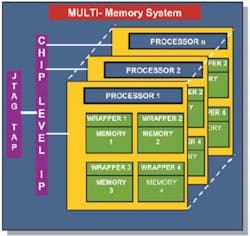
The multiple engines that test and repair groups of memories must be connected to each other and the chip�s IEEE 1149.1 JTAG port to provide access to the chip for external test equipment for diagnosis and debugging. This requires a chip-level IP infrastructure that is design aware, has intimate knowledge of the memory and test and repair groups, and acts as a chip-level IP infrastructure hub (Figure 2).
IP Integration
With the explosion of memories on-chip, chip designers no longer can manually integrate the test and repair logic into the RTL for their design, which is a cumbersome and error-prone process. Architects and designers also frequently change their minds during a design cycle. Any design changes resulting in swapping memories in and out could trigger a new RTL and a new insertion, resulting in the same time-consuming manual process. For that reason, a capability to not only generate all the pieces of the solution, but also to integrate them in the design is required to enhance productivity. Such a capability must be intimately aware of the embedded memory test and repair architecture and allow insertion, deletion, and modification of the memory test and repair solution at the SOC level.
Not all memory test and repair logic is inserted at the same level of the hierarchy, and such a capability must manage the inclusion of various components at different levels of hierarchy. This capability automates the management of the design hierarchy and makes ECOs faster.
Putting It All Together
Conventional memory and third-party bolt-on BIST solutions are outdated. The third-party BIST solution is not intimately aware of the memory topology and has no knowledge of process defect history, so the BIST algorithms are generic and can lead to test escapes.
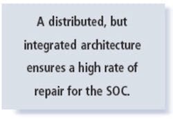
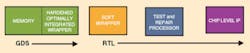
The right architecture for today�s advanced designs is one in which the repairable memories are preconfigured with the appropriate number, type, and location of spare elements; the common noncritical test and repair functions are centralized within a test and repair processor; and the critical test and repair functions are incorporated into an optimally integrated wrapper (Figure 3). In addition, an infrastructure IP to coordinate and manage chip-level test functions and an insertion capability to manage the overall design hierarchy are musts.
The distributed, but integrated architecture ensures a high rate of repair for the SOC and short test times as well as optimized area and maximum performance. The overall yield dramatically improves the company�s bottom line.
About the Author
Krishna Balachandran is senior director of product marketing at Virage Logic. Before joining the company six years ago, he spent several years in the EDA industry working at Cadence, Synopsys, and Gambit. Mr. Balachandran has a master�s degree in computer engineering from the University of Louisiana and an executive MBA from Stanford University. Virage Logic, 47100 Bayside Parkway, Fremont, CA 94538, 510-360-8000, e-mail: [email protected]
FOR MORE INFORMATION
on embedded memory test and repair
www.rsleads.com/507ee-192
July 2005
About the Author
Comment About the Article
To join the conversation, and become an exclusive member of Electronic Design, create an account today!

Leaders relevant to this article: