Lead-Free Reliability Issues and Test Methods
Environmentally friendly is a term rapidly invading the electronics industry.
The electronic industry will be facing great challenges over the next few years as the solder used in electronic products is migrating toward lead free. This is being driven by mandates in Europe such as Waste Electrical and Electronic Equipment (WEEE) and Restrictions of Hazardous Substances (RoHS) and similar ones in Japan. There also is a great deal of pressure in the United States to do the same.
Many electronic component suppliers have or will be phasing out their parts used for tin-lead solder. The new components made for lead-free solder will have different finishes on the leads than those used for tin-lead solder. If that is not enough reason to change to lead-free solder, some of your competitors already may be producing electronic products with lead-free solder and using this as a strong competitive marketing tool. Furthermore, there is and will be ever-increasing pressure to be environmentally friendly.
Changing to lead-free solder is a very significant move. After all, solder is the glue that holds electronic products together. We have successfully used tin-lead solders for years and have good engineering knowledge about their reliability. Now we must change this most fundamental and important building block.
We also must make certain that the lead-free product is just as reliable as the one that has been using tin-lead solder for years. We must ensure that it is reliable for use in sometimes-critical applications with very demanding environments. And, we must do this without the benefit of long-term engineering or product experience with lead-free solder.
Reliability Issues of Lead-Free Solder
Broad lead-free vs. tin-lead solder reliability trends cannot be assumed. The creep-fatigue models for lead-free solder are not fully developed at present.
Published test results comparing the reliability test life of lead-free vs. tin-lead solder are inconsistent. Many different variables including solder alloy mixes, solder fluxes, board finishes, manufacturing process variables, component finishes, packaging, and test variables such as stress type, temperature range, and dwell time affect the testing. The results are test and product specific.
Lead-free solders have a higher melting point than tin-lead solders. Many lead-free solder alloys feature a melting point above 215�C compared to 179�C to 188�C for tin-lead solders.
Lead-free solders have poorer wetting characteristics than tin-lead solders, which increases the risk of solder defects. This means that much higher process temperatures must be used to melt lead-free solder for longer durations to overcome the poorer wetting characteristics. These harsher process conditions may cause damage to the circuit board and the electronic components and reduce product reliability.
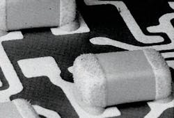
Lead-free solder is susceptible to failure modes such as tin whiskers, Kirkendall voids, and mechanical shock. Tin whiskers can grow from tin-based finishes on components and connectors in a lead-free solder joint (Figure 1). A whisker is a thin cylindrical growth or filament. These whiskers are brittle and can break off or bridge across solder joints to cause electrical shorts.
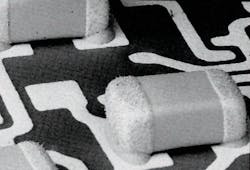
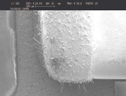
Tin-whisker growth is aggravated when there are compressive stresses in the tin plating. Ironically, lead was added to the tin to mitigate whiskering in the past.
Some precautions can be taken to help avoid whisker growth such as not using tin plating, stress relieving or annealing the components with tin plating, and using conformal coatings. At present, there is no absolute recipe to avoid tin whiskers�except to not use tin plating�because this phenomenon is not fully understood. Test results have shown that tin whiskers can be grown as a result of temperature cycle tests and constant temperature/humidity tests.
Kirkendall voids are caused by intermetallic growth between two dissimilar metals, specifically tin and copper in a lead-free solder joint. Intermetallic growth is caused by diffusion of one material into another.
The diffusion between copper and tin is unbalanced which causes Kirkendall voids to occur. These voids can accumulate and reduce the strength of the solder joints. Kirkendall void growth can be aggravated by accelerated aging at a high constant temperature.
Many lead-free solder alloys are stiffer or less ductile than tin-lead solders. This is an area of concern for highly stressed vibration environments and mechanical shock conditions.
Also, many lead-free solder alloys lose their ductility very abruptly at approximately -30�C. This transition temperature is affected by different alloy blends and becomes very important when used in outside applications such as automotive or aerospace.
In addition, the possibility exists for reliability issues prompted by lead contamination in lead-free solder joints, especially those containing bismuth. This may occur when using a lead-free alloy to solder a component with tin-lead plated leads. The lead may accumulate and form voids that will weaken the solder joint. The mechanical fatigue strength could be reduced by as much as 50% with as little as 0.5% weight contamination. Some thermal cycling test results also show significant life reductions.
Reliability Testing
A typical circuit board may contain hundreds of solder joints with many different types of components. So how do you ensure that your lead-free product will remain reliable in its intended use?
A comprehensive reliability test program is a must. Start with a highly accelerated life test (HALT) using a HALT chamber. HALT chambers can apply rapid thermal ramp rates and random vibration in 6-degrees-of-freedom simultaneously.
Sometimes a one-day rapid HALT is beneficial to get preliminary reliability information. The HALT can be started at the circuit-board level with special fixtures as shown in Figure 2. After the HALT has been completed successfully at the circuit-board level, a verification HALT can be performed on the assembled product.
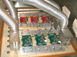
It also is important to perform the HALT on a sample of both lead-free and tin-lead boards. This can be performed simultaneously if space permits or as two separate tests.
Perhaps the product with tin-lead solder already has completed HALT so just the new lead-free product will have to undergo HALT. Still, it is very important that a HALT be performed on both lead-free and tin-lead products to ensure that the lead-free product is as reliable as the tin-lead product or until unrealistic temperatures are reached.
By starting with HALT, reliability results can be obtained within days instead of waiting weeks for accelerated reliability tests. A HALT is a qualitative step stress test.1 The stresses will be increased until operating and then destruct limits are found.
In addition, HALT uses combined temperature, vibration, and electrical stresses so your lead-free product will be exposed to multiple types of stresses during one test. Why spend weeks of accelerated reliability testing if HALT shows immediately that your new lead-free product does not perform as well as your existing tin-lead product?
Since the lead-free solder-joint reliability issues are broad, it is risky just to perform HALT or just one type of accelerated environmental test. The overall test plan depends on the product type and application. A product that will be used outdoors will have a different test program and test levels than a product in an office environment.
Vibration tests are performed to test a product�s tolerance to vibration in automotive or aeronautical applications. Random spectrums typically are used during vibration tests using an electrodynamic (ED) shaker. Durations generally are one hour or more per axis.
Mechanical shock and drop tests are completed to determine the solder joint�s capability to withstand rough handling environments. Shock is a high-intensity, short-duration impulse load.
Shock or drop simulations usually are performed on special shock tables, ED shakers, or drop testing machines. The number of pulses could range from a few to many depending on the product�s intended use. Classical shock pulse types are haversine, half-sine, saw-tooth, square, and trapezoid.
Vibration and mechanical shock tests usually are performed at ambient temperatures. For combined effects, a HALT or ED shaker with an Advisory Group on Reliability of Electronic Equipment (AGREE) type chamber typically is used.
Temperature testing involves cycling a product between high and low temperatures. These tests usually are performed in single-compartment chambers at rates of 20�C/minute or less. The maximum and minimum temperatures and the total number of cycles depend on the product and its application.
Lead-free solder requires greater dwell times during thermal cycling to produce the same amount of fatigue damage that would occur to tin-lead solders. For that reason, a different accelerated-temperature cycle test using longer dwell times must be performed for lead-free solder.
There are various opinions on the minimum dwell times required during temperature cycle tests for lead-free solder. Figure 3 suggests an optimum dwell time of 10 minutes is most efficient for lead-free assemblies using Sn-Ag-Cu (SAC) alloys; however, longer dwell times technically are valid.2 This data is specific for ceramic ball grid array (CBGA) components mounted on FR-4 circuit boards cycled between 0�C to 100�C.
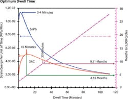
Figure 3. Dwell Time Comparison of Lead-Free (SAC) vs. Tin-Lead (SnPb) for CBGA Components Mounted on FR-4 Circuit Boards
Reprinted with permission from EPSI
These optimum dwell-time results should not be extrapolated broadly. Also, the dwell times should be measured on the product and not the incoming chamber air. This may require longer dwells in the chamber profiles to achieve the proper dwell times on the product.
Thermal shock tests are performed to determine a product�s resistance to extremely rapid temperature changes. Thermal shock tests normally are conducted in single-compartment liquid nitrogen-cooled chambers or multicompartment chambers where the product is moved rapidly between hot and cold compartments.
As a rule, thermal shock tests are performed at a rate of 30�C/minute or greater. In thermal shock, higher stresses and less creep occur in the solder joints; in thermal cycle tests, lower stresses and more creep occur.
Different failure modes probably will occur in the solder joints during thermal shock vs. thermal cycle tests. This is true for both lead-free and tin-lead solder joints. Thermal shock tests may not be appropriate for every product.
Constant temperature or humidity tests are conducted to determine a product�s susceptibility to thermal aging, humid environments, and extended use at cold temperatures. These tests are conducted in single-compartment chambers under ambient atmospheric pressure.
Sometimes, a highly accelerated stress test (HAST) can be performed to significantly shorten the time required for humidity testing. HAST is performed in a special chamber that provides noncondensing humidity at temperatures higher than 100�C and pressures greater than atmospheric. It usually achieves the same failure modes as an 85�C/85% RH test conducted under normal atmospheric pressure.
These are the most commonly performed tests to determine the durability of both lead-free and tin-lead solder joints. Other specific tests are completed depending on applications.
During these reliability tests, the solder joints typically are monitored by event detectors that continuously check the electrical resistance of the solder joints or use comprehensive functional testing. After reliability testing, the solder joints should be examined under magnification for tin whiskers, cracks, and defects.
Conclusion
There are many challenges to ensure that your lead-free electronic product will be as reliable as its tin-lead solder predecessor. Lead-free solder reliability depends on many variables such as solder alloy composition, manufacturing process variables, circuit board packaging, assembly, and reliability test conditions.
A comprehensive program with multiple tests is a must to reduce the risk of early reliability failures in lead-free products. One reliability test is not enough. Only time will tell whether your new lead-free product will be as reliable as the existing product using tin-lead solder.
References
1. Hobbs, G. Accelerated Reliability Engineering: HALT and HASS, 2000.
2. Clech, J.P., �Acceleration Factors and Thermal Cycling Test Efficiency for Lead-Free Sn-Ag-Cu Assemblies,� paper presented at 2005 SMTA International.
About the Author
Gary Delserro, P.E., is president of Delserro Engineering Solutions. He has more than 20 years of experience in the field of stress optimization and reliability working for the Naval Air Warfare Center as an aerospace reliability engineer, Cooper Industries as a new product/R&D manager, and Mack Trucks as a senior durability/reliability test engineer. Mr. Delserro holds a B.S.M.E. from Villanova University and an M.S.M.E. from Lehigh University. Delserro Engineering Solutions, 3900 Broadway Rd., Easton, PA 18040, 610-253-6637, e-mail: [email protected]
June 2006
About the Author
Comment About the Article
To join the conversation, and become an exclusive member of Electronic Design, create an account today!

Leaders relevant to this article: