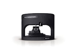
High-accuracy tip, sample heater augment nanomechanical property measurement
Santa Rosa, CA. Keysight Technologies has announced the availability of a high-accuracy tip and sample heater to expand the utility of its Nano Indenter G200. This easy-to-use solution uses a precise high-power diode laser to heat the sample and the indenter tip.
Benefits include the ability to measure nanomechanical properties at precisely controlled temperatures and to test a wide range of samples under highly dynamic temperature conditions. To ensure reliable data, the system minimizes drift associated with heating by using function-optimized materials and an adjustable laser spot size. Keysight Nano Indenter G200 users also have the option to purge samples with various gases to avoid contamination and oxidation.
The new tip and sample heater for the G200 supports a wide temperature range (RT up to 500°C) and is accurate to within 0.1°C. Another advantage is the high rate of the system’s heating and cooling processes. Depending on the temperature, the rate can exceed 20 K/s in either direction. This capability affords scientists and engineers many new and intriguing opportunities for dynamic materials testing.Keysight’s laser-heated indenter tip, a critical component of the new system solution, prevents disturbance of the substrate temperature during measurement. This stability is critical for working with materials that have poor thermal conductivity and whose mechanical properties are strongly affected by temperature. Keeping the tip and sample at the same temperature as one another also allows G200 users to perform high-temperature continuous stiffness measurements with exceptional precision.
The Nano Indenter G200 system’s substrate holder is optimized to provide high mechanical and temperature stability. To ensure simple and convenient G200 operation, the transparent plate underneath the sample contains a built-in thermocouple. When the absolute highest accuracy is needed, such as for nanoindentation applications involving thick polymer samples, users can mount a thermocouple to the sample surface. The dual-loop PID controller’s NanoSuite interface offers complete NanoSuite software integration.
About the Author

Rick Nelson
Contributing Editor
Rick is currently Contributing Technical Editor. He was Executive Editor for EE in 2011-2018. Previously he served on several publications, including EDN and Vision Systems Design, and has received awards for signed editorials from the American Society of Business Publication Editors. He began as a design engineer at General Electric and Litton Industries and earned a BSEE degree from Penn State.

