Nova-Microchip Team Up on Battery-Management Reference Platform

What you'll learn:
- Microchip Technology and Nova Semiconductor have joined forces to develop a complete, pre-validated reference platform for a battery-management system.
- The new platform will pair Nova’s NB1600 battery-management system (BMS) silicon with Microchip’s industry-proven MCUs and firmware ecosystem.
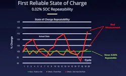
- The BMS is expected to provide highly precise state-of-charge tracking with simultaneous cell and current measurement at high accuracy (1 mV, 0.02% SOC repeatability).
Nova Semiconductor recently announced that it’s collaborating with Microchip Technology to deliver a complete, pre-validated reference platform for a battery-management system (BMS). The solution pairs Nova’s NB1600 BMS silicon with Microchip’s MCUs and firmware ecosystem.
Nova’s NB1600 simplifies battery-management architecture by pre-integrating many specialized functions required to achieve advanced functionality. Microchip provides the MCU hardware and the core firmware stack required to manage and control the system.
Key technical capabilities of the combined reference architecture include:
- Complete battery-management functionality, with minimal firmware development effort.
- Simultaneous cell and current measurement with high accuracy (1-mV measurement, 0.02% SOC repeatability) for highly precise state-of-charge tracking.
- Dedicated ADC and reference per cell to ensure maximum signal integrity.
- An on-chip electrochemical impedance spectroscopy (EIS) system for real battery systems.
- Reduced integration risk with a solution that helps simplify safety-oriented design decisions, fault handling, and system validation.
- Support for functional-safety goals with an architecture that helps the BMS detect faults early, communicate critical events, and take timely protective action.
Next in This Edition of PowerBites
 dreamstime_3ddock_20723988_promo
More PowerBites

 powerbites_promo
About the Author
 Lee Goldberg
Lee Goldberg
Contributing Editor
Lee is the author of the popular PowerBites series.
Lee Goldberg is a self-identified “Recovering Engineer,” Maker/Hacker, Green-Tech Maven, Aviator, Gadfly, and Geek Dad. He spent the first 18 years of his career helping design microprocessors, embedded systems, renewable energy applications, and the occasional interplanetary spacecraft. After trading his ‘scope and soldering iron for a keyboard and a second career as a tech journalist, he’s spent the next two decades at several print and online engineering publications.
Lee’s current focus is power electronics, especially the technologies involved with energy efficiency, energy management, and renewable energy. This dovetails with his coverage of sustainable technologies and various environmental and social issues within the engineering community that he began in 1996. Lee also covers 3D printers, open-source hardware, and other Maker/Hacker technologies.
Lee holds a BSEE in Electrical Engineering from Thomas Edison College, and participated in a colloquium on technology, society, and the environment at Goddard College’s Institute for Social Ecology. His book, “Green Electronics/Green Bottom Line - A Commonsense Guide To Environmentally Responsible Engineering and Management,” was published by Newnes Press.
Lee, his wife Catherine, and his daughter Anwyn currently reside in the outskirts of Princeton N.J., where they masquerade as a typical suburban family.