A Guide on LVS in the Nanometer Era

Layout versus schematic (LVS) is a method to validate that the layout of an integrated circuit is functionally identical to the original schematic of the design. LVS debug of today's nanometer era designs isn’t only challenging, but also time-consuming. Therefore, reducing the LVS debug time while continuously delivering reliable, high-performance design is a requirement for chip designers who want to meet their tight tapeout deadlines and go beyond client expectations.
To ensure the correctness of the implemented design, bigger layout databases need to be checked during the physical verification stage in the same ambitious project time frames as before.
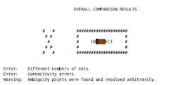
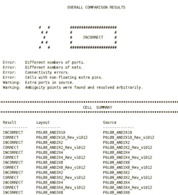
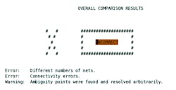
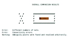
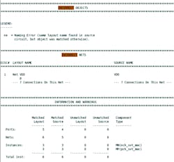
The LVS report describes the comparison between the layout and schematic with respect to ports, nets, and instances. If the schematic and the layout don’t match, the discrepancies are mentioned, separated by broken lines. The “overall comparison results” gives the numerical details of the ports, nets, and instances appearing in the layout and schematic (also referred to as source).
The report gives detailed information on the sources of error either in the layout or schematic by displaying the comparison results. All of the errors can be tracked by understanding the LVS report, thus avoiding any design failure that could lead to expensive mask changes and delays in getting the system-on-chip (SoC) to market.
LVS, which is a part of physical verification, checks whether the design layout is equivalent to its schematic and checks the layout against process manufacturing guidelines provided by the semiconductor fabrication labs to ensure it can be manufactured correctly. LVS verifies the design correctness with intended functionality, and formal verification matches the design’s pre-layout netlist to post-layout netlist.
These “sanity checks” should be done before running LVS:
- The design doesn’t have any signal or power short/open.
- The design doesn’t contain any overlapping of cells.
- The design db. and Open Artwork System Interchange Standard (OASIS) should have syn.
- The design doesn’t have a base layer DRC.
LVS Flow
An electronic-design-automation (EDA) tool performs LVS via a set of instructional code input, commonly known as an LVS rule deck, which is a guide for the verification tool to provide the instructions and identify files that are needed for LVS.
Design inputs needed for running LVS are:
- OASIS or Graphical Database System (GDS) layout database of the design
- Schematic netlist of the design (Spice netlist)
- LVS rule deck file (SVRF/TVF)
- LVS options file provided by foundry
- LVS IP filter file provided by foundry
- Source layout netlist ($design.netlist.layout)—the LVS tool creates a layout netlist by extracting the geometries
LVS is a two-step process:
- Extraction: The process extracts the devices and their connectivity from the physical layout, and then generates a netlist interpretation of the layout to be used in the comparison step.
- Comparison: The process compares the extracted netlist to the schematic netlist, and reports all discrepancies, which must then be debugged and resolved.
If extraction isn’t clean, the subsequent compare results may be invalid because many of the errors reported in the LVS results will turn out to be extraction errors rather than true comparison errors. Even if the extraction errors are removed, debugging and resolving the true LVS discrepancies at advanced technology nodes can be difficult and may seriously impact the total turnaround time of a project.
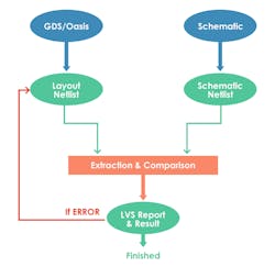
The steps in the LVS flow include (Fig. 1):
- GDS/OASIS: The tool takes the GDS (or OASIS) file as input and breaks it down into basic design devices like transistors, diodes, capacitors, resistors, etc.; it recognizes the devices in the form of layers and shapes that make up the circuit. It also extracts the connectivity information between these devices from the GDS file.
- Layout netlist: Device information along with their connectivity is written into a layout netlist file. It also contains physical cells, generally called layout extracted netlist. This process is known as extraction.
- Schematic netlist: This netlist is a textual description of a circuit that contains components like gates. It also has a connection with the resistors, capacitors, and transistors.
- Comparison: This tool compares the electrical circuits from the schematic netlist and the layout extracted netlist and reports all discrepancies, which must then be debugged and resolved. The netlist comparison process also uses the LVS rule deck.
- LVS report & result: If the two netlists differ, discrepancies are reported in the form of an LVS result database that can be used to debug LVS issues. The result database would contain the list of incorrect elements and the reason for mismatch, such as incorrect nets, incorrect ports, and incorrect instances.
LVS Issues and Debug
The LVS report describes the comparison between the layout and schematic with respect to ports, nets, and instances. If the schematic and layout don’t match, the discrepancies are mentioned, separated by broken lines. The “overall comparison results” gives the numerical details of the ports, nets, and instances appearing in the layout and schematic (also referred to as source).
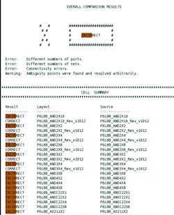
LVS Overall comparison result shows discrepancies (incorrect matching) in the following points:
- Number of nets
- Number of ports
- Connectivity issues
- Ambiguity points in the design
- Cell comparison
How to Open LVS db. in Calibre
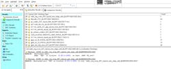
First you have to check latest OASIS file of your current db. Then from below command you can invoke caliberDrv (Fig. 2):
calibredrv -64 $design.oasis_file{Oasis file of design}
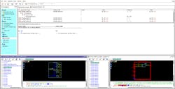
How to open LVS marker:
- Verification -> Start RVE (Fig. 3). Then give the option to be lvs and subsequently give the pointer to calibre/lvs/svdb.
- Then check for discrepancies (Fig. 4).
- Debug layout missing connections and plot error with them.
Case 1: Short
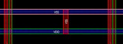
Shorts between different nets are the most common problem during the final tapeout. Fixing those shorts is one of the toughest challenges for the designers.
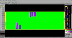
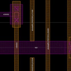
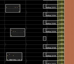
When two different nets’ layers touch each other, it will result in a short in your design. Shorts can also occur when in a specific layer of GDS, two polygons having different layout text overlap and have no intersection. In the example in Figure 5, two signal nets are creating a short between each other in db.
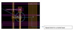
In general practice, in the place-and-route tool we need to fix shorts before running LVS, one short present in PNR tool is showing in the above figure.
Possible of shorts include:
- Short between full chip-level net and block level.
- Short between P/G inside block level or between full chip and block nets.
- Signal/PG short during merging hierarchical design.
- Short between DM and signal/PG nets.
Once Calibre LVS has run the LVS process and generated a shorts database, the results are displayed in Calibre RVE, a result viewing tool (Fig. 6).
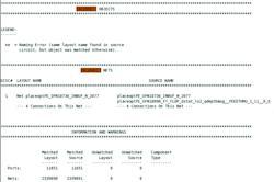
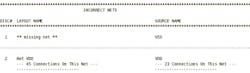
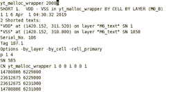
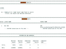
In the LVS report, the number of nets in the source is greater than that in the layout (Fig. 7). If a short is present in a design, then the connectivity extractor will only extract the shorted nets as a single net in the layout and will not be able to identify them as two different nets (Fig. 8).

Case 2: Power Short
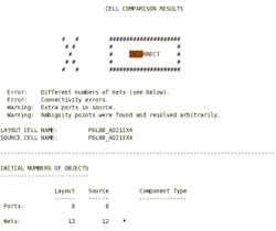
Power shorts are actual connectivity issues that have been analyzed and found to be a short by the comparison process (Fig. 10). Designers can begin debugging these comparison errors, and load Calibre RVE to see a visual representation of the layout and source netlists used in the LVS run, and debug LVS discrepancies by comparing the source and layout schematics side-by-side.
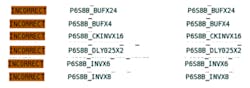
If your design has power short, then you must clean it in place-and-route before moving in signoff—otherwise, you might face a number of issues in LVS. It’s tough to debug power short in lvs. In Figure 11, the overall comparison of design is showing an error and an alternate instance is showing incorrect because of the power short.
Further in the report, it shows a missing net of VSS because the tool under the VDD and VSS nets appears as one net due to a short (Fig. 12). The tool will generate a short.rpt report for the short as well (Fig. 13).
When the layout net count is greater than source netlist in the net section, then shorts exist in the design. If it’s a valid short, the tool will dump the report. Shorts file into the Calibre results directory (Fig. 14).
Case 3: Power Open
An open in a design occurs when polygons having the same layout text aren’t connected to each other, or when two nets having same net names aren’t connected to each other.
Note: It’s suggested that the open/Short script always run in the place-and-route tool before running LVS to detect the open/short in the early phase of the design cycle.
Even LVS will not show power open. Instead, it will show CORRECT because ERC verifies the correctness of power and ground connections, so this will not reflect in LVS.
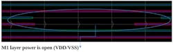
In Figure 15, LVS shows that the example VDD and VSS nets got open.
Case 4: Power Short with Signal
Shorts are formed if two or more wires that should not be connected together become connected. Figure 16 shows a case where power VDD is getting shorted by one of the signal nets. Figure 17 reveals the LVS detailed errors.
When the source net count is greater than the layout netlist in the net section, then shorts exist in the design (Fig. 18).
Case 5: Signal Open
Opens are formed if the wires or components that should be connected together are left floating or are partially connected. An open in a design may result in floating gates, which leads to short-circuit power dissipation and may even lead to chip failure.
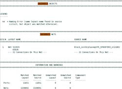
In the example in Figure 19, two signal nets got open. The LVS report details these errors (Fig. 20).
When there’s a lesser net count at the source side compared to the layout side (Fig. 21), then an open exists in the design.
Case 6: Particular Instance is Deleted
This issue arises when a designer is in a manual fixing cycle and accidentally deletes the particular instance, and subsequently moved ahead. This is because the LVS algorithm only works on whatever netlist received by the user. If your source netlist doesn’t contain x instance, it will not create a layout for that particular instance and hence the comparison process will not detect the issue.
In this case, lvs will not detect this issue and it will show CORRECT. This is because it will work on the netlist that’s dumped from your latest database—if an instance is deleted an instance from the latest database, it will not reflect in the layout netlist.
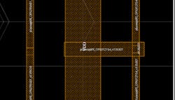
Case 7: Missing Well Tap
Figure 22 illustrates a missing well tap. Tap cells are used to provide a substrate connection; they connect an n-well to VDD and p-sub to VSS. These cells are inserted in the layout at regular intervals based on tap rules (tap-to-gate distance) defined in the technology rule deck file.
If we missed these cells, n-well continuity will stop and due to that, the instance of a row (that’s not continuous) will not get power (VDD) (Fig. 23). The report in Figure 24 shows that particular instance as incorrect.

As shown in the report in Figure 25, again there’s a lesser net count at the source side compared to the layout side. In addition, an open of VDD exists in the design, highlighted by the incorrect instances in the LVS report.
Case 8: Overlapping Filler Cells in db.
This situation arises when a designer is in a manual fixing cycle and placement filler cells became overlapped with each other. Thus, we have to run LVS with the same db. But LVS will not detect this issue and give you clean results.
Case 9: Missing Filler Cells in db.
If you forgot to add filler into your design and gone through LVS, then it will be hard to detect this issue in an LVS report because every alternative cell is showing incorrect due to N-well discontinuity. It will fail ERC (electrical rule check) and give floating n-well violations (Fig. 26).

Basically, filler cells will provide power/ground and n-well continuity. There will be power/ground opens between the standard cells (empty space), creating incorrect cells in the report (Fig. 27). As a result, not every cell will have power/ground connectivity, making it an incorrect cell.
Conclusion
The article covered some of the general debugs that are used when you need to analyze LVS results. If we debug LVS step by step, it will help us understand the error in depth, and the GUI mode will help to understand depth of the mismatch. Using this corner case can be helpful in physical-verification iterations for debugging the LVS.
Chetna Jaiswal is Senior Engineer, Sandeep Jain is Technical Lead, and Mrunal Mirani is Physical Design Engineer at eInfochips.
About the Author
Chetna Jaiswal
Senior Engineer, eInfochips
Chetna Jaiswal is a senior engineer at eInfochips. She holds a Bachelor of Engineering degree in Electronics and Communication from SAIT, Indore, India and has five years of experience in the lower technology node for complex networking SoCs. She has developed expertise in PnR and static timing analysis.
Sandeep Jain
Technical Lead, eInfochips
Sandeep Jain is Technical Lead at eInfochips. He holds a Bachelor of Engineering degree in Electronics and Communication from Government Engineering College, Ajmer, India. He has six years of experience in physical designing and has developed expertise in physical verification and static timing analysis.
Mrunal Mirani
Physical Design Engineer, eInfochips
Mrunal Mirani is Physical Design engineer at eInfochips. He holds a Bachelor of Engineering degree in Electronics and Communication from MEFGI, Rajkot, India. Presently, he is doing Block Level Implementation for a networking ASIC chip using 7-nm FinFET technology, where his accountabilities include the block level APR and complete sign-off closure for the same.
Comment About the Article
To join the conversation, and become an exclusive member of Electronic Design, create an account today!

Leaders relevant to this article: