Select the Right Flash Memory for Your Battery-Powered AI Speaker with Voice Control

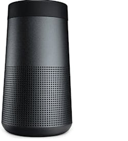
A popular implementation of artificial intelligence (AI) is a battery-powered smart speaker with voice control (Fig. 1). The device is voice-activated, responding to a wakeup word like “Allegra,” “Odessa,” or “Adesto.” Once awake, a virtual assistant handles further voice commands.
Unlike many similar devices currently on the market, the goal for the smart speaker described here is to keep average power consumption low enough to allow the device to run from batteries. It should not be required to be connected to external power all of the time. It therefore needs to be a power-efficient AI system.
To understand how such a smart speaker operates, let’s examine the overall system. AI relies on two distinct modes of operation: the learning phase, which is where the system learns the characteristics of the types of data it’s operating on, and the inference phase, where the system is using what it has already learned to interpret new data.
The learning phase consists of feeding the system large amounts of known data and building up a set of inference tables as the output. This requires a lot of computing horsepower and/or time. For an edge device, the learning phase isn’t done on the device itself. It’s done “once and for all” on a large computer system, and the resulting inference tables are stored as fixed data tables in the edge device.
The inference phase is the word-recognition phase. This is repeated every time the device is receiving new data. For the wakeup phase, for instance, it’s listening to a spoken word and using the inference tables stored on the device to determine if the word it just heard was its magic wakeup word.
A Core Issue
Real-time AI algorithms require a great deal of CPU horsepower, so our system needs a large, powerful CPU with lots of memory. At the same time, users want long battery life, so the system must have ultra-low energy consumption while the AI algorithms are trying to detect the wakeup word. Users also expect immediate response from the device once they speak their command word. The part of the system that recognizes the wakeup word therefore needs a very fast response time.
All of these requirements are difficult to achieve with just one CPU core and one memory system. Using two or more cores, with different memory systems, is likely a more cost-efficient solution. These may be two separate MCUs or a single-chip system-on-chip (SoC) with a multi-core CPU.
The main CPU could be a single MCU, a multi-core CPU, an AI accelerator, a GPU, or any combination of these. The amount of memory required ranges from a few hundred megabytes to several gigabytes. Systems that are limited to handling only a few spoken commands are able to operate on much less memory.
In the configuration shown in Figure 2, the main CPU will handle the bulk of the local AI processing. It may also call up to the mothership in the cloud as needed. In our example, much of the heavy processing will not take place inside the smart speaker itself, but in a remote system server in a data center.
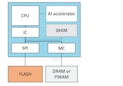
In this configuration, the CPU will boot from external flash (large NOR or NAND non-volatile memory) and execute from the faster external DRAM or PSRAM. To save power, the main CPU will be turned off when not in use and the power-hungry DRAM and SRAM memories will be powered off while the device is in sleep mode.
The main CPU will only be woken up after the wakeup word has been received and recognized. This necessarily means that there will be a certain delay each time it wakes up to reload the memories.
Always-On CPU
While the main CPU is sleeping, and during the time it takes the main CPU to reload its memories, the always-on CPU will be in charge. The main task of the always-on CPU is to listen to incoming sounds, detect and recognize the wakeup word, and then alert the main CPU as required. At a minimum, it will require enough AI capability to recognize a single spoken word. Once it detects the right word, it will wake up the main CPU and let the big guy take it from there.
The always-on CPU may also handle other tasks that don’t require advanced AI; for instance, housekeeping and audio playback. This means that the main CPU can be put back to sleep relatively fast, while the always-on CPU holds the fort. The amount of memory the always-on CPU requires to handle its simple tasks is much less than what’s required for the main CPU.
The always-on CPU may also be turned off when not in use, provided it can wake up quickly enough. For instance, it may sleep until the microphone detects sound, but must be able to start executing fast enough to catch the beginning of a spoken word.
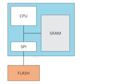
This makes it difficult to use a boot+SRAM (Fig. 3) as the memory configuration for the always-on CPU. The amount of memory required for AI applications means on-chip SRAM would be expensive, and the response time requirement means that there’s no time to reload the memory. The SRAM would have to be kept on all of the time, resulting in high power consumption. To reduce SRAM size, it would be possible to keep only the code in SRAM and keep the AI inference tables in flash. But this option would still consume power.
Embedded flash (Fig. 4) could handle the wakeup time requirement, but it has drawbacks.
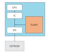
The non-volatile code storage is on the same die as the CPU, which saves both time and power. However, the large memory requirement is expensive. In addition, using embedded NVM means that the always-on CPU can’t be put on the same die as the main CPU because the main CPU is typically too large to be implemented in an embedded NVM process. Or, if we really wanted to keep both CPUs on the same die using an embedded NVM process, the main CPU would be considerably more expensive than necessary.
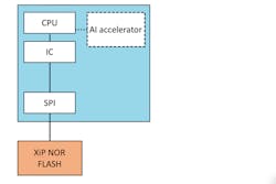
XiP Memory
Using an execute-in-place (XiP) memory as code storage is the most viable option for the always-on CPU. In an XiP configuration (Fig. 5), the CPU is built with an instruction cache (IC). Every time the CPU fetches an instruction, it will first check in the cache memory to see if that address location has already been loaded into the device. If it has, the CPU will load the instruction from cache, and if not, it will start a read operation from the flash to fill the missing cache line.
Even though an XiP system uses a separate die for flash, it has many of the same features as an embedded flash device. The standby or sleep power can get down to the same sub-microampere range as embedded flash devices. At the same time, the wakeup times will be in the range of microseconds to a few milliseconds, just like systems using embedded flash.
In AI applications, the inference engine needs to go through a large number of NVM-stored coefficients in a very short time and with minimal power consumption. The data sets are too large to fit in the cache, so the raw bandwidth of the interface between the flash and the host controller becomes the critical factor for maximum performance.
Getting an XiP solution implemented correctly is not that easy if you try to use standard flash for this purpose. For decades, the main purpose of standard flash devices has been to serve as boot memory for shadow flash systems. While these memories have been optimized to serve that application very well, they fall short in their use as XiP memory.
Specifically, as XiP memory, standard serial flash delivers much lower performance than one would want to see, and the power consumption is high in both operational and sleep modes. Standard flash can only run at 104 or 133 MHz in SDR mode (SDR is single-data-rate mode, sometimes referred to as single-transfer-rate or STR mode). Even when running in a quad mode, the peak throughput is limited to 52 or 66 MB/s.
Applying an Octal DDR Interface
This is where an octal DDR interface, such as Adesto’s EcoXiP, really shows a difference compared to a quad SPI device. EcoXiP is an application-specific non-volatile memory with throughput up to 300Mbytes/s, as well as low cost and low power consumption for microcontroller designs using an execute in place architecture.
EcoXiP is designed from the ground-up with XiP systems in mind, and specifically targets low-power operation. It supports high-speed data speed transfer in both octal and quad modes and offers dual and single data rates for both. Additionally, EcoXiP has functions designed to provide better latency and throughput for cached CPU architectures.
A unique feature offered by EcoXiP is concurrent read and write with no additional delay on the read operations. If a program or erase operation has been started in one part of the memory, the device can still read from another part of the memory without any delay. This significantly simplifies data-logging operations and over-the-air updates for devices without on-chip program memory.
Summary
For AI applications on the edge, the performance and cost of the system will depend directly on the performance and cost of the memory. External DRAM is too power-hungry, external quad SPI flash is too slow, and internal embedded flash is too small or too expensive.
XiP memory as code storage is clearly the best option for the always-on CPU of AI systems. With no embedded NVMs on either of the CPUs, it’s then easy to add both to the same die and create an SoC.
For more detailed information on these memory configurations, check out the whitepaper "AI on the Edge: Don’t forget the Memories.”
Bard M. Pedersen is Director of Technology at Adesto.
About the Author
Bård M. Pedersen
Director of Technnology, Adesto Technologies Corp.
Bård M. Pedersen has over 20 years of experience in the electronic systems and semiconductor industries. As Director of Technology at Adesto, he is responsible for technology development and new product definitions, and has been responsible for technical marketing, reference designs, and applications support.
His technical expertise includes non-volatile memories; microcontroller-based embedded systems; analog, digital, and mixed-signal design; LED drivers; design for EMC compatibility; and embedded software development. More than a decade in applications design and support has made him an ardent problem solver.
Bård received his Master’s in Electrical Engineering from the Norwegian Institute of Technology (NTNU), Norway. He holds several patents in memory-related technologies.
Comment About the Article
To join the conversation, and become an exclusive member of Electronic Design, create an account today!

Leaders relevant to this article: