Download this article in PDF format.
Use of surface-mount technology (SMT) in consumer products offers a major competitive advantage—they enable significant design miniaturization. Surface-mount devices (SMD) come in a variety of standard packages like the miniature 0201 and 01005, as well as SOT, SIOC, QFP, and BGA packages.
OEMs can either make their products smaller or integrate more features into the same product size. However, one critical aspect of successfully using such small components in any product is the ability of the contract manufacturer to handle these components using their manufacturing equipment.
Handling small SMT components successfully requires tight process windows. For instance, the current process control for 0402-size components is Cpk (capability process index) greater than 1.5 along with a specification window of 150 µm. For 0201-size SMT components, a Cpk over 2.0 is the minimum requirement along with a specification window the size of 100 µm. With high-volume manufacturing, the control may require a tighter specification window size of 75 µm.
The ability to apply adequate amounts of solder paste to the board also impacts the placement quality. If the CM prefers to maintain their current printing practices, they may have to pay attention to the effect of powder size. Powder size and placement accuracy has an impact on the manufacturing quality when SMT components have sizes of 0201 and 01005.
Concerns Over Use of Small SMT Components
In the electronic industry, OEMs have some universal concerns and some unique concerns over the use of small SMT components (see table).
However, certain technical factors are driving the electronics industry to adopt small SMT parts such as 0201 and 01005. One of them is the increased usage of large, fine-pitch ball-grid arrays (BGAs)—forcing OEMs to use 0201 with BGAs rather than the preferred 0402. Another technical factor is the industry’s need for space—utilizing small SMT components leads to either a reduction of the product size or high density favorable to mobile devices and hearing aids. High-speed applications also benefit from the use of small SMT parts, as the tiny packages have very low parasitics.
On the other hand, some technical factors also limit the use of small SMT components. Most often, OEMs don’t use small components as their product line doesn’t require components that small. Some OEMs do not employ small SMT parts because they’re not confident of the reliability of 0201 and 01005 size of components. Other OEMs cite the increased cost and CM inability for not using small SMT components. Some OEMs prefer to forge ahead with the 0402 size of components, since they can fit micro-vias in these pads.
Handling Small SMT Components
Efficient handling of small SMT components requires defining, optimizing, and controlling following parameters:
- Design of mounting pads
- Proper circuit trace width
- Design of solder mask
- Proper stencil for solder-paste deposition
- Proper solder-paste selection
- Accuracy of placement
- Proper selection of thermal profile for reflow soldering
- Final inspection of solder joints
Design of Mounting Pads
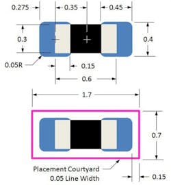
Component manufacturers recommend the optimum design of mounting pads for their components (Fig. 1).
Circuit Trace Width
For 0201 and 01005 SMT components, the pad is very small and the width of the trace plays an important role. Due to the small size of the pad, the solder on the pad tends to form a bump, allowing the component to slide down on one of its sides—this may result in the component tilting.
Designers prevent tilting by using a PCB trace with width equal to the width of the mounting pad. As molten solder reflows, the excess amount runs down the trace, thereby reducing the overall thickness of solder under the component, limiting its tilting. Designers control the length of the solder wicking by controlling the solder-mask opening on the mounting pad. Check out some of factors affecting print quality of SMT solder paste by clicking here.
Design of Solder Mask
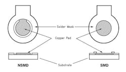
Designers usually follow one of two methods of designing the solder mask for small SMT components—non-solder mask defined (NSMD) and solder mask defined (SMD). While NSMD pads have the solder mask skirting the copper pad, SMD pads have the solder mask overlapping the copper pad (Fig. 2).
For SMD pads, the presence of solder mask controls the flow of molten solder and limits it to the top of the copper pad, preventing it from overflowing down the sides of the pad. For the NSMD pad, there’s no such restriction and the molten solder is free to flow both across the top and down the sides of the copper pad.
We recommend the use of NSMD pads over SMD pads because it’s easier to define and control the size of a copper pad compared to the opening of the solder mask. Typically, the copper-etching process has a higher tolerance capability than that of the process controlling the solder mask. It’s also easier to visually inspect the solder fillet of an NSMD pad.
Stencil for Solder-Paste Deposition
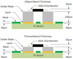
Thickness of the stencil is very important when depositing solder paste for small SMT components, as it defines the volume of solder paste deposited on the board. Although the opening may remain the same, a thicker stencil will deposit a higher volume of solder paste because of greater height. The excess solder paste may overflow during reflow, causing solder bridging (Fig. 3).
We recommend using stencils of around 0.1 mm (4-5 Mils) thickness for 0201-size components. The design of the stencil must ensure tapering sidewalls of the openings at about 5 degrees. For smooth discharge of solder paste after removal of the stencil, laser-cut openings are necessary, and the sides of the opening must have an electro-polish finish.
We also recommend using jet paste printers rather than stencils for solder-paste deposition. Jet paste printers are especially useful for PCBs using small SMT components, as users can program the printer to deposit a specific amount of solder paste for each pad. Users can monitor in real-time and adjust the coverage area, height, volume, and layers of solder paste the jet printer is depositing.
Solder-Paste Selection
Type IV powder size in solder paste containing 90% solids works best for soldering small SMT components. One can use either no-clean or water-soluble solder-paste formulations.
Thermal Profile During Reflow
Depending on the multiple packages present on the board during reflow, it’s necessary to verify the thermal profile for all new board designs, especially if the board has 0201 and 01005 components. Usually, the profile provided by the solder manufacturer is the starting point with minor adjustments made on account of the flux.
Rush PCB recommends not raising the temperature of the PCB at a rate faster than 2°C when it’s in the pre-heat zone. How long the PCB remains in the soak zone depends on the time it takes for the solder to thoroughly expel flux remnants, and the risk of voiding.
Summary
A significant portion of the modern component market now represents 0201 and 01005 SMT components, and it’s progressively growing larger. At present, wider adoption of these components depends on manufacturability issues, cost of use, and inspection of assembled boards. With certain industries driving the increase in adoption based on a trend for smaller products, it’s resulting in improved manufacturing practices.
Akber Roy is the CEO of RUSH PCB Inc.About the Author
Akber Roy
CEO, RUSH PCB Inc.
Akber Roy is the CEO of RUSH PCB Inc. Akber Roy has 20 years of experience of electronic contract manufacturing. RUSH PCB’s website provides detailed printed-circuit-board development resources.
