Checking Out Lattice’s Embedded Vision Kit
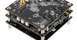
Lattice Semiconductor’s Embedded Vision Development Kit (EVDK) is only $199 (Fig. 1), at least until the end of 2018. It consists of three boards: a Crosslink VIP board, an ECP5 VIP processor board, and an HDMI VIP Output Bridge board. This FPGA-based solution takes advantage of the Modular Video Interface Platform (VIP) for embedded vision. It’s an ideal platform for developing and experimenting with high-performance video processing for applications such as drones, augmented reality, and Industry 4.0 machine vision.
1. The Embedded Vision Development Kit incorporates a CrossLink VIP board, an ECP5 VIP processor board, and an HDMI VIP Output Bridge board.
The CrossLink VIP Input Bridge board includes two Sony IMX 214 high-speed MIPI D-PHY interface camera sensors. The ECP5 VIP Processor board holds an ECP5-85 FPGA that’s optimized for image signal processing. Replete with an on-board USB programmer, it handles most of the custom work. The HDMI VIP Output Bridge board provides support for HDMI displays.
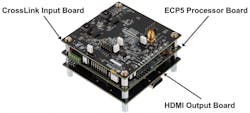
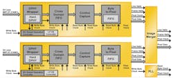
The EVDK is just part of Lattice’s solution targeting vision applications. Its SensAI stack features tools that incorporate machine learning (ML), including FPGA-based binarized-neural-network (BNN) and convolutional-neural-network (CNN) accelerators (Fig. 2). BNNs target the compact, iCE40 UltraPlus FPGA, while the CNN support addresses the ECP5 FPGA. The SensAI neural-network compiler can take Caffe and TensorFlow models and generate weights for FPGA IP.
2. The EVDK is the basis for Lattice’s SensAI solution for vision processing.
The EVDK is supported by Helion Vision’s Helion IONOS Image Signal Processing (ISP) IP (Fig. 3). A free evaluation version of Helion IONOS ISP support is included with the EVDK. This includes 9- to 32-bit color support with video-processing support such as lens shading correction and defective pixel correction. These tools are typically used to clean up or optimize the video data.
3. Helion Vision’s Helion IONOS Image Signal Processing support is free with the EVDK.
Helion has over 100 cores that come preconfigured. These can be combined and managed using a common configuration bus that’s configurable via a microcontroller. Helion provides a graphical configuration application that streamlines development. IP blocks are able to be chained together, and each can be individually configured.
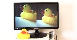
4. The EVDK comes programmed with an application that takes the two camera inputs and streams the combined video information to a single HDMI display.
The EVDK comes programmed with an application that exercises all of the major components. It takes the inputs from the two cameras and combines the video streams to a displayable single stream (Fig. 4). The HDMI VIP Output Bridge board is designed to connect directly to an HD display. Checking out the demo software takes only a few minutes, since it’s only a matter of plugging in the HDMI cable and the supplied power brick. To illustrate further, here’s a demo from Lattice:
The next step takes a bit more time. I had to download Lattice’s Diamond software development platform and install it, but first Windows 10 had to update itself. Not to be delayed, I submitted my request for the free one-year license via email. That showed up a day later. On the plus side, you can start this process before the kit arrives. I just wish the Windows 10 updates would work properly. I spent more time having it revert to a previous version and then manually installing an update than I did getting Diamond installed with a new license file.
Now the hard work starts as FPGA development is still a chore. The development tools have improved significantly over the years, and access to the Helion ISP support makes the job much easier. Still, consider just the starting point for the demo project. This includes a pair of image-processing blocks (Fig. 5).
5. The demo application includes a pair of image-processing blocks that are then merged into a single stream.
This merged stream is then handed off to the Helion ISP blocks (Fig. 6). The blocks include pixel correction, white balance, debayer, color space conversion, and gamma correction. For the demo, these blocks use the default settings, but this is a place where developers can easily experiment with settings as well as include additional blocks within the data stream. The output is sent to the HDMI board that can hand it off to the HD display.
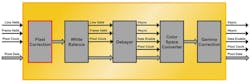
6. The data stream is passed through a bunch of Helion blocks to clean up the video stream.
Moving past the initial demo and into development isn’t like dropping off a cliff. Lattice has free IP and reference designs on its site. Most include very good documentation, although each instance is often targeted at a specific platform. For example, Face Tracking Using Convolutional Neural Network Accelerator IP is a reference design for the EVDK, although it requires the addition of an inexpensive MicroSD adapter board (Fig. 7). The documentation is over a dozen pages and it details the architecture, Verilog HDL, and Diamond project.
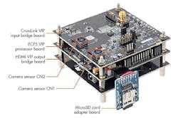
7. The Face Tracking Using Convolutional Neural Network Accelerator IP is a reference design that targets the EVDK.
The project takes advantage of the SensAI support, including the use of the CNN accelerator. Check out the Lattice Neural Network Compiler for more details.
Changing the architecture of the system will require a bit of learning if you’re not familiar with Verilog or the Diamond tools. However, adjusting the CNN model used in the system is relatively straightforward.
FPGAs, vision systems, and machine learning remain a challenging development space, but platforms like the EVDK are making it significantly easier to get started.

About the Author

William G. Wong
Senior Content Director - Electronic Design and Microwaves & RF
I am Editor of Electronic Design focusing on embedded, software, and systems. As Senior Content Director, I also manage Microwaves & RF and I work with a great team of editors to provide engineers, programmers, developers and technical managers with interesting and useful articles and videos on a regular basis. Check out our free newsletters to see the latest content.
You can send press releases for new products for possible coverage on the website. I am also interested in receiving contributed articles for publishing on our website. Use our template and send to me along with a signed release form.
Check out my blog, AltEmbedded on Electronic Design, as well as his latest articles on this site that are listed below.
You can visit my social media via these links:
- AltEmbedded on Electronic Design
- Bill Wong on Facebook
- @AltEmbedded on Twitter
- Bill Wong on LinkedIn
I earned a Bachelor of Electrical Engineering at the Georgia Institute of Technology and a Masters in Computer Science from Rutgers University. I still do a bit of programming using everything from C and C++ to Rust and Ada/SPARK. I do a bit of PHP programming for Drupal websites. I have posted a few Drupal modules.
I still get a hand on software and electronic hardware. Some of this can be found on our Kit Close-Up video series. You can also see me on many of our TechXchange Talk videos. I am interested in a range of projects from robotics to artificial intelligence.
Comment About the Article
To join the conversation, and become an exclusive member of Electronic Design, create an account today!

Leaders relevant to this article: