Make the Move to Machine Learning, Neural Networks for CMP Modeling
Machine learning (ML), neural networks (NNs), and deep learning have many applications in different areas of modern industry and life. Their ability to “learn” how to analyze and predict imprecise data has dramatically improved the state-of-the-art in areas of speech recognition and language translation, genomics and drug discovery, computer vision, autonomous vehicles, and many others.1
One potential new use in the semiconductor industry is the application of ML and NNs to post-deposition surface profile modeling. While there are no “unimportant” steps in integrated-circuit (IC) production, chemical-mechanical polishing (CMP) has reached an unprecedented level of criticality in the IC manufacturing process. With designs so tightly packed and scaled down to the most advanced process technology nodes, post-CMP planarity variations can now have a significant impact on manufacturing success.
With different materials exhibiting different erosion rates under the CMP process, it’s essential to maintain a constant density balance across the die to prevent any bumps and dishing that can cause shorts and opens in the metal interconnects. Most IC manufacturers use some type of CMP modeling to detect potential CMP hotspots in front-end-of-line (FEOL) and back-end-of-line (BEOL) layers as part of their design-for-manufacturing (DFM) flow.
The introduction of high-k metal-gate (HKMG) technology with additional CMP steps,2,3 the high cost of lithography due to double and triple patterning, strong depth-of-focus (DOF) requirements, and improved accuracy of CMP models have all increased interest in CMP modeling4-7 as a way of finding and resolving potential CMP issues before manufacturing.
Building a CMP Model
CMP modeling has a long history in IC design and verification.7 CMP modeling measures various aspects of the layout in an attempt to maintain even planarity as the chip is built up over multiple layers, and looks for areas of the design that have a higher-than-average probability of experiencing defects post-CMP. The main concept behind CMP modeling is to extract geometrical properties of the pattern on the layout, generate a pre-CMP surface profile after etch and numerous deposition steps, and predict the post-CMP surface profile for different patterns on the layout.
First, a chip is divided into tiles of fixed size. Each tile represents a trench with given geometric characteristics (such as width, space, pattern density, and perimeter) and data for two heights that define the height of material inside the trench (ZT) and outside the trench (ZNT). For each tile, the average geometric characteristics of a pattern are extracted and passed to etch, deposition, and CMP simulation processes. An effective trench approximation is used to model the structure defined for each tile (Fig. 1).
1. Chips are divided into tiles, and each tile’s geometric characteristics are extracted and passed to etch, deposition, and CMP simulation processes.
During CMP simulation, etch, deposition, and polishing models simulate the change in ZT and ZNT data, as well as the geometry data change for each tile. The first polishing step always uses the post-deposition profile as input.
The polishing model employs pre-CMP surface-profile data as input, which is generated by either a deposition model or data from a previous polishing step. The surface profile after deposition isn’t planar and contains variations. To generate the correct input profile for CMP simulation and ensure high-quality CMP modeling results, it’s vital to have a set of deposition models that correspond to the deposition processes used by manufacturers.
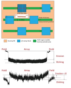
An essential step in CMP model building is to use measurement data from test chips. A CMP test chip usually consists of periodically placed array blocks of parallel trenches of different widths with differing spaces between them. The size of the test chip and the number of structures must be selected in a way that provides good coverage of the width, space, perimeter, and pattern density values supported by the technology node, without violating design rule checks (DRC). An atomic force microscope (AFM) scanner or other profiler tool is often used to collect erosion and dishing data from line scans over test patterns (Fig. 2). By knowing the layer stack information and material thicknesses, design teams can convert erosion and dishing data into ZT and ZNT surface-profile heights data.
2. AFM (or other scanner) line scans are used to collect erosion and dishing data from a CMP test chip.
Generation of a high-quality pre-CMP surface profile is crucial for accurate CMP model building, due to the complicated nature and long-range effects of CMP. Even with advanced deposition processes, the post-deposition (pre-CMP) profile on a patterned wafer is non-uniform, and may contain large variations that can affect on-surface planarity after CMP. Analysis of three-dimensional (3D) AFM and transmission electron microscopy (TEM) data shows a complicated pre-CMP profile height dependence on the underlying pattern geometry for the following deposition processes:
- High-density plasma CVD (HDP-CVD)
- Spin-on dielectric (SOD)
- Flowable CVD (FCVD)
- Enhanced high-aspect-ratio processes (eHARP)
Shallow trench isolation (STI) and CMP modeling of FEOL layers shows successful application of HPD-CVD and SOD deposition models to CMP modeling. However, building physics-based or compact models for FCVD and eHARP processes is more challenging, since these processes include several deposition and annealing steps to fill up trenches.
The FCVD process, developed by Applied Materials,8 deposits a high-quality dielectric film in a liquid-like state on the wafer surface. This allows the film to readily flow into the gap, filling it completely and without voids or seams.
eHARP is a non-plasma-based CVD oxide film deposition process that addresses the gap-filling requirements for STI at the 4xnm node and beyond.8 The eHARP process may be used before HDP-CVD to fill narrow trenches.
Both of these processes are too complicated for building a physics-based or compact model with a reasonable runtime and accuracy for CMP modeling. Seeking an alternative solution, we decided to investigate the use of ML algorithms in conjunction with NNs to create CMP models.
CMP Modeling with Machine Learning and Neural Networks
To test the practicality and accuracy of using ML and NNs to generate CMP models, we experimented using the following four deposition processes: HDP-CVD, SOD, FCVD, and eHARP. We started with HDP-CVD and SOD processes, for which compact models were available. We extracted local geometric characteristics of a pattern (width, space, pattern density, and perimeter) from the layout (for simplicity, any geometry change after deposition wasn’t considered).
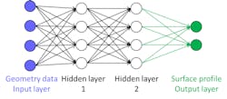
3. A multi-layer feed-forward neural network with two hidden layers was determined to be optimal for the required modeling.
Using measured data, we generated a training set to use for NN training to generate surface-profile height data predictions on an output layer (Fig. 3). Erosion and dishing data were collected from AFM line scan data from the test chip, and a training data set (see table) constructed for NN input.
We considered an NN with one, two, and more hidden layers for fitting erosion and dishing data. We determined that for our model, two hidden layers are optimal for modeling the surface profile of the mentioned processes (Fig. 3, again), and there’s no need to use deeper architectures (i.e., an NN with many hidden layers).
We then trained the NN using an advanced learning algorithm with a training set constructed of measurements collected from CMP test chips after deposition. Next, the trained NN was run on a test chip or production designs for testing and validation. To obtain good generalization of the model to unknown data, best practice is to start from a minimum number of hidden layers and neurons, and increase them continuously to get better fitting on validation data (while avoiding over-fitting).
Subsequently, we performed validation on measured data and simulated data generated by models for the HDP-CVD and SOD processes. Finally, we applied the NN to modeling of pre-CMP profiles for FCVD and eHARP processes.
Results
HDP-CVD process modeling
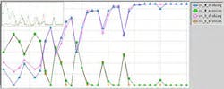
Figure 4 shows fitting of 150 sites of the training set with a NN of two neurons per hidden layer. An absolute error per site is less than 3%. Due to the small fitting error, the simulated and measured data are indistinguishable on the plot.
4. The HDP-CVD erosion and dishing data fitting during NN training showed an absolute error per site of less than 3%.
Next, we ran a model validation using a different CMP test chip. Figure 5 displays the fitting of erosion and dishing data of the NN model versus compact model data for 33 structures. The error of fitting erosion and dishing data is larger than for the training set. As expected, the error is larger for the input values that are farther from the values used for training. Because the NN model isn’t physics-based, it may report non-physical results like small negative dishing, or erosion for some narrow or wide trench sites. While it’s safe to set these data to zero, in general, this may be avoided if a large-enough data set is used for training.
5. In model validation, the HDP-CVD validation error per site is about 10%, and for some sites, dishing error is about 40% (error subplots aren’t in scale with the fitting plots).
We observed that the NN model prediction has 98-99% correlation with compact model data, and the root-mean-square (RMS) error is roughly equivalent to the measurement error. The NN model predictions are in good agreement with both AFM line scan data and the HDP-CVD compact model.
SOD process modeling
For NN modeling of the SOD surface, a NN with two hidden layers and four neurons per hidden layer (Fig. 3, again) was trained on a training set of 145 sites (Fig. 6).
6. The SOD process erosion and dishing fitting during training shows good fitting of measured data.
The validation of the model was done on a different CMP test chip with SOD compact model simulated data for 35 sites (Fig. 7). Here, also, the overall data fitting looks good except for a few sites, which can be corrected by extending the training set with more data.
7. In the SOD model validation, the validation error per site is less than 5%, and for some sites, erosion error is about 50% (error subplots aren’t in scale with the fitting plots).
FCVD process modeling
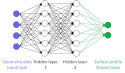
An NN consisting of two hidden layers with six neurons per layer is used for modeling surface profiles after FCVD (Fig. 8).
8. A multi-layer feed-forward neural network with two hidden layers and six neurons per hidden layer was selected for modeling surface profiles after FCVD.
In Figure 9, fitting of erosion and dishing data of the FCVD process on a training set with 163 measured data is shown.
9. The FCVD process erosion and dishing data fitting during training shows good fitting of measured data.
Correlation of dishing and erosion data on a validation set with 38 sites is 98% and 95% respectively (Fig. 10). The average error is about 15-20%.
10. During FCVD model validation, the correlation of simulated versus measured dishing and erosion data was 98% and 95%, respectively (error subplots aren’t in scale with fitting plots).
eHARP process modeling
We used an NN to model the HDP-CVD surface profile after eHARP, since it’s the profile that’s used for CMP modeling (Fig. 11). We used the same NN configuration we used as for the FCVD process. Training was done by fitting of erosion and dishing data on a training set with 61 measured data.
11. The HDP-CVD post-eHARP process training fit of erosion and dishing data used a training set with 61 measured data.
Figure 12 shows the validation set with 18 measurements with error subplots. The average error is about 10-20%.
12. The post-eHARP model validation returned an average error of about 10-20% (error subplots aren’t in scale with fitting plots).
Conclusion
The application of ML and feed-forward NNs to post-deposition surface profile modeling of advanced deposition processes presents an exciting opportunity to develop accurate CMP models for complex CMP processes.
In our experiments, a simple feed-forward NN with two hidden layers and a small number of neurons on the hidden layers was successfully used for surface-profile modeling of HDP-CVD, SOD, FCVD, and eHARP deposition processes, with more than 95% correlation and a small error per site. The challenge of using an NN is that the NN model isn’t physics-based, and it may report non-physical results (like small negative dishing) for some patterns that aren’t expected for the given deposited processes.
In the modeling presented here, simple correction was done. In the future, though, a special activation function must be used. Using NNs for the modeling of geometry data change after the deposition process simultaneously with heights data is straightforward. The challenge here is to get geometry data from AFM line scans or other measurements for the training data set. In principle, it may be done, but it will require a more detailed analysis of measurement data.
Based on the results of our research, the application of NNs to deposition profile modeling looks promising, and it’s under active investigation.
Ruben Ghulghazaryan is Lead R&D Engineer and Jeff Wilson is DFM Product Marketing Manager at Mentor, a Siemens Business.
References:
1. Y. LeCun, Y. Bengio, G. Hinton, Deep Learning, Nature 521, 436 (2015).
2. K. Mistry, C. Allen, et al., “A 45nm Logic Technology with High-k+ Metal Gate Transistors, Strained Silicon, 9 Cu Interconnect Layers, 193nm Dry Patterning, and 100% Pb-free Packaging,” IEEE International Electron Devices Meeting, Washington D.C., 247 (2007).
3. M. Krishnan, J. W. Nalaskowski, and L. M. Cook, “Chemical Mechanical Planarization: Slurry Chemistry, Materials, and Mechanisms,” Chem. Rev. 110, 178 (2010).
4. U. Katakamsetty, D. Koli, Y. Sky, H. Colin, R. Ghulghazaryan, B. Aytuna, J. Wilson, “20nm CMP Model Calibration with Optimized Metrology Data and CMP Model Applications,” Proc. of SPIE Vol. 9427, doi: 10.1117/12.2085728 (2015).
5. U. Katakamsetty, J. J. Chee, et al., “Cutting-edge CMP modeling for front-end-of-line (FEOL) and full stack hotspot detection for advanced technologies,” Proc. of SPIE Vol. 10148, 101480Q (2017).
6. R. Ghulghazaryan, J. Wilson, A. Abouzeid, “FEOL CMP Modeling: Progress and Challenges,” Proc. of ICPT 2015, 34 (2015).
7. R. Ghulghazaryan, J. Wilson, N. Takeshita, “CMP Model Building and Hotspot Detection by Simulation,” Proceedings 158th Meeting of Planarization CMP Committee, 55 (2017).
8. Producer® Eterna™ FCVD™, http://www.appliedmaterials.com/products/producer-eterna-fcvd
About the Author
Ruben Ghulghazaryan
Lead R&D Engineer
Ruben Ghulghazaryan is a lead R&D engineer in the Design to Silicon division at Mentor, a Siemens Business. He has extensive experience in both theoretical and applied physics research, with numerous industry and academic publications. He received a M.Sc. in Theoretical Physics and Biophysics at Yerevan State University and a Ph.D. in Physics from Yerevan Physics Institute.
Jeff Wilson
DFM Product Marketing Manager
Jeff Wilson is a DFM Product Marketing Manager in the Calibre organization at Mentor, a Siemens Business. He has responsibility for the development of products that analyze and modify the layout to improve the robustness and quality of the design. Jeff previously worked at Motorola and SCS. He holds a BS in Design Engineering from Brigham Young University and an MBA from the University of Oregon.
