Top 5 Secrets of High-Speed PCBs Revealed by Professionals
This article is part of the TechXchange: PCB Tools and Technology
What you’ll learn:
- Designing high-speed PCBs.
- Maintaining signal integrity for faster signal transmission.
- Reducing crosstalk in high-speed PCBs.
Vigorous competition in the electronics market means developers must keep modification in mind when designing systems. High-speed PCBs are increasingly important to high-performance solutions, but high-speed PCB assembly is costly. That's why you can’t experiment with these boards or generate a lot of prototypes. This article offers five tips to help streamline and improve those high-speed PCB designs while keeping costs at bay.
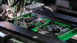
1. Design of the assembly
High-speed assembly needs some additional components compared to any other type of PCB assembly, such as conventional or rigid-flex assembly. These components change according to every application's need, but all must be given extra care during the manufacturing phase. The main factors that professionals keep in mind during development include:
• Noise is a very big factor to consider. Minimize the noise production from the source generating the power, as well as the switch noise that’s generated due to the continuation of the power supply.
• The crosstalk between traces must be cut off.
• The consequence of ground bounce must be reduced.
• Termination of signal lines must be considered.
• Make sure impedance matching is proper.
2. Designing in the board material and transmission line
The noise generated in the PCB is mainly due to the dielectric material used as the component to make the board. It also causes crosstalk signal generation. The high-frequency signal directly impacts the PCB due to the high absorption and high frequency of its dielectric material.
Signal transmission also affects the performance of the signal and the noise generation. The physical features of trace tracks, such as the width, length, and thickness, affect the PCB and the separation between the traces. Professionals typically use two routes for circuit trace layout: microstrip transmission and stripline transmission.
Microstrip transmission works on the outer layer of the PCB, while stripline transmission works on the inner layers of multilayer PCB. The characteristics of both are nearly identical except for speed. Microstrip is much faster than stripline when it comes to a shift in trace separation.
Impedance is a crucial component to consider when developing a high-speed PCB prototype.
3. Reduce the crosstalk
Crosstalk reduction of nearby signals is important because disturbances will cause interference. It must be applied in microstrip and stripline transmission. Steps to reduce the crosstalk include:
• Try to minimize the gap between the signal by managing them, thus prohibiting routing.
• Place transmission lines very close to each other toward the ground citation plane.
Try various routing methods for important networks.
• Perform route signaling.
Parallel signaling is important to some extent, but in the long run, route signaling is necessary. However, route signaling is nothing but a collection of short parallel trace signals.
4. Maintain signal integrity
The integrity of the signal is essential so that the signal is consistently delivered from its source to destinations in the PCB assembly. A high-speed PCB signal is generally a one-ended signal. To achieve the best outcome from a one-ended signal, follow these rules:
Don't use many single layers.
In the trace, don't use vias.
• For layout, use microstrip or stripline only.
• Lessen the reflection of the signal.
• Try to maintain a steady area between the signal to avoid crosstalk.
5. Filtering and grounding of the PCB
Filtering works well to avoid the noise in high-speed PCBs. A capacitor can be used in this case—it filters the noise with low frequency.
For a high-speed assembly, grounding is a crucial factor. Ground bouncing is a flexible feature that regulates the switching of ground voltages. In high-speed PCBs, ground bouncing can be mitigated/removed by using one of these methods:
• Position the vias near the capacitor and unite them with trace.
• Connect the power with small traces.
• Put in a decoupling capacitor and place it near the IC.
• Never exceed the buffer load against the capacitor load.
• Apply surface-mount technology to reduce the capacitance.
Conclusion
When venturing into high-speed PCB assembly manufacturing, you may run into several new problems that need quick resolutions. However, if you follow the guidelines above, which are maintained by professionals, you can easily handle such issues.
About the Author
Ken Ghadia
Senior Sales Engineer, TechnoTronix
Ken works as Sales Engineer at Technotronix. He brings 15 years of experience in PCB sales and technical client services.
Comment About the Article
To join the conversation, and become an exclusive member of Electronic Design, create an account today!

Leaders relevant to this article: