4D LiDAR Sensors on a Chip
This article appeared in Machine Design and has been published here with permission.
A collaboration announcement between Aeva Technologies and Nikon Corporation marks a moment of growth, as they expand the use of LiDAR technology into the industrial automation, metrology, and manufacturing space.
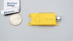
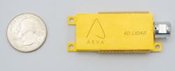
Aeva, a Mountain View, Calif.-based LiDAR company, will leverage its unique perception technology with micron-level measurement capability and Nikon’s high-precision industrial automation and metrology capability. The collaboration to develop next-generation industrial solutions marks the first time Aeva’s 4D LiDAR technology is used outside of self-driving cars.
“We’re excited to work closely with a leader like Nikon in an established market with massive growth potential as we accelerate our expansion into industrial applications, targeting product release in 2025,” said Soroush Salehian, co-founder and CEO at Aeva.
Salehian said his company’s LiDAR chip architecture, or frequency-modulated continuous wave (FMCW) 4D LiDAR, has the potential to upend the growing industrial automation industry. The software stack will enable the company to scale into such industries as industrial robotics, consumer electronics and healthcare. The solution is smaller and cheaper than comparable industrial sensors, he said.
Light Detection and Ranging
LiDAR stands for “Light Detection and Ranging.” LiDAR sensors measure the time it takes for the light to bounce off objects. The distance between the object and the sensor is measured and creates a map of an environment. Legacy or time-of-flight LiDAR measures only depth and reflectivity. FMCW LiDAR streams continuous beams of light to objects in an environment and measures velocity, depth reflectivity, and inertial motion.
Salehian explained that Aeva’s 4D LiDAR-on-chip measures distance as well as instant velocity of every point on objects without losing range. The FMCW technology operates at fractions of the optical power required at this range. A notable differentiator has been the ability to integrate multiple beams on a single chip, said Salehian. Each beam can measure more than 2 million points per second at distances beyond 300 m.
The technology already plays a pivotal role in the emerging automated driving industry, particularly for advanced driver-assistance systems (ADAS) and autonomous driving systems. Aeva developed its technology for OEM and automotive firms and has received strategic investments from Porsche SE, and secured relationships with large Tier 1 automotive suppliers. In January, Aeva collaborated with Denso, a global mobility supplier of advanced automotive technology for automakers, to bring Aeva’s 4D LiDAR technology to the mass vehicle market.
About the Author

Rehana Begg
Editor-in-Chief, Machine Design
As Machine Design’s content lead, Rehana Begg is tasked with elevating the voice of the design and multi-disciplinary engineer in the face of digital transformation and engineering innovation. Begg has more than 24 years of editorial experience and has spent the past decade in the trenches of industrial manufacturing, focusing on new technologies, manufacturing innovation and business.
Her B2B career has taken her from corporate boardrooms to plant floors and underground mining stopes, covering everything from automation & IIoT, robotics, mechanical design and additive manufacturing to plant operations, maintenance, reliability and continuous improvement.
Begg holds an MBA, a Master of Journalism degree, and a BA (Hons.) in Political Science. She is committed to lifelong learning and feeds her passion for innovation in publishing, transparent science and clear communication by attending relevant conferences and seminars/workshops.
Comment About the Article
To join the conversation, and become an exclusive member of Electronic Design, create an account today!

Leaders relevant to this article: