A Spectrum of EDA Functionality is Essential for PCB Design Workflows

This article is part of the TechXchange: PCB Tools and Technology
What you’ll learn:
- Why PCB workflows need different levels of EDA functionality.
- How to use the right amount of EDA for different PCB tasks.
- Which PCB scenarios require maximum vs minimum EDA.
Designing a PCB is a complex undertaking, but there’s no such thing as any one best way to approach the job. Sometimes engineers want to take a “quick and dirty” approach and just get an idea out of their head to see if it works. Other times, they want to get “down in the weeds” and use every electronic design automation (EDA) tool at their disposal.
To be able to approach PCB design workflows in their preferred manner—and avoid being shoehorned into a predetermined way of working—engineers need access to a full spectrum of functionality that runs the gamut from “minimal EDA” to “maximum EDA.” It’s a bit of a Goldilocks situation: Ensuring there’s not too much EDA, and not too little, but just the right amount, depending on the task at hand.
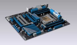
Consider the three following scenarios, which are illustrative of the different tasks an engineer might face in the process of creating a PCB (see figure) and how they might tackle them most efficiently.
Task #1: Quickly and Easily Testing a Layout
Sometimes, an engineer wants to skip the schematic process and build their prototype right from scratch as a board design. They know what they want—it’s in their head. The goal is simply to lay something out and see if it works rather than going through the whole traditional schematic process. If—after testing the layout—it works, then they can hand it off to a team member to generate a schematic.
Having that capability significantly cuts down the design time for the engineers who like to work this way, since they know what they have in their head and likely don't want to do anything more detailed than scratching it out on a napkin. This is a case where the old adage is true: Sometimes less is more. Additional functionality would only cramp their style for this particular task.
Task #2: Exporting Bond Wire or Creating Decals
In certain scenarios, engineers don’t need full on EDA, but they do need the ability to “dip their toes” into the EDA waters a bit. In these scenarios, it’s helpful to have more advanced bits of functionality off to the side that engineers can easily make use of as dictated by their workflow preferences.
For instance, by having access to a standalone bond-wire exporter solution, designers can start with a simple DWG file that has lines, arcs, polylines, and other design elements representing bond wires from a chip to a substrate. They can then use the bond-wire exporter to “intelligize” the DWG and output the file to a bond-wiring machine. This is ideal for the designer who wants to create only graphic representations of a chip design.
Likewise, there might be people who don't utilize EDA, but still need translators for Gerber, or for decals and GDS for other design elements. When this functionality is broken out as a standalone option, it can support these niche workflows without overwhelming engineers with more functionality than they need.
Task #3: Working with Thick Film
Some tasks require full EDA, and processing thick-film ceramic designs is one of them. It requires tools such as an enhanced dynamic masks generator, panel generation, and ODB++ output, in addition to bond-wire data export to support bond-wire machines.
These tools—in addition to nibbler data for removing cavity material in bulk or in steps, and control of the Gerber, hole, and punch data for correct output to manufacturing—are beneficial for low- and high-temperature co-fired ceramic design.
The ability to work with thick film is particularly beneficial because more and more manufacturers are switching over to it. It’s simply cheaper to manufacture thick film than it is to continue supporting processes like low- and high-temperature co-fired ceramic design. You can count the number of big companies that are still producing LTCC and HTCC materials on one hand.
Having the tools to effectively work with thick film, then, is more than just a matter of getting the job done in a preferred manner. It’s a matter of staying with the times and adapting to shifting macrotrends within the industry.
Something for Everyone
What the above scenarios make clear is that there’s no such thing as “one size fits all” when it comes to PCB design. Sometimes a “light touch” is what’s needed to tackle a task most efficiently; other times, it requires “industrial strength” EDA capabilities.
For their part, software vendors need to ensure that they have a strong enough foundation to be able to offer engineers the tools that fit their workflows across any of these scenarios, delivering just the right amount of EDA functionality.
Once they have these tools in hand, engineers can tackle the various aspects of PCB design in the way that makes the most sense for them. Because while the end products may be very similar, the approach to designing them should be anything but that.
About the Author
Tom Dlouhy
Technical Director, CAD Design Software
Comment About the Article
To join the conversation, and become an exclusive member of Electronic Design, create an account today!

Leaders relevant to this article: