Low-Power FD-SOI FPGA Melds AI and Bridging
Lattice Semiconductor is well-known for its low-power, flash-based FPGAs. One of the applications the company has targeted is interfacing between devices. The CrossLink-NX FPGA is designed to provide such bridging support with built-in, hard IP serial interfaces supporting devices like digital cameras. The FPGA fabric can be used to handle protocol conversions, but it’s also capable of implementing more complex machine -earning (ML) models to process data (Fig. 1).
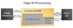
This type of implementation can be very useful in automotive applications where radar, LiDAR, or vision sensor data streams can be processed by the FPGA instead of having it done on the host. Of course, hosts with ML support are being used as well, but the low-power nature of the CrossLink-NX enables designers to build more power-efficient systems.
CrossLink-NX and Lattice’s FPGAs in general have a soft error rate (SER) that’s up to 100X lower than similar FPGAs in its class due to two factors: they are flash-based, and the implementation of Lattice’s transistor technology. This is important for safety and high-reliability applications. The initial set of CrossLink-NX devices targets ruggedized environments found in outdoor, industrial, and automotive applications.
The design of CrossLink-NX is built around three key elements. The chips include hard IP blocks that deliver fast I/O support to handle interfaces such as MIPI, PCIe, and DDR3 memory. The flash-based nature of Lattice’s FPGA families allows for instant-on operation. CrossLink-NX I/O configuration can be done in less than 3 ms and total device configuration takes less than 15 ms. Finally, the CrossLink-NX family has a high memory-to-logic ratio. This is designed to address ML inferencing. The family features 170 bits of memory for every logic cell.
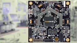
The CrossLink-NX family comes in a very small form factor—devices are available in 6- × 6-mm packages.
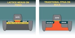
CrossLink-NX is built on Lattice’s new Nexus platform that’s based on 28-nm, fully depleted silicon-on-insulator (FD-SOI) technology. The FD-SOI support from Samsung cuts transistor leakage in half compared to bulk CMOS (Fig. 2).
“We are excited to collaborate with Lattice to bring the benefits of our Samsung Foundry 28FDS manufacturing process technology to the low-power FPGA market,” said Ryan Lee, Vice President of Marketing at Samsung Foundry. “By combining their innovation and expertise in FPGA fabric design with our industry-leading and differentiated foundry technology, Lattice will continue its leadership in low-power FPGAs for years to come.”
Radiant 2.0
Also included in Lattice’s latest announcements is release of Lattice Radiant 2.0, their FPGA software design tool. Radiant supports all of Lattice’s FPGA families including the CrossLink-NX.
Roger Do, Senior Product Line Manager, Software, at Lattice said, “Lattice Radiant 2.0 design software gives developers an easy-to-follow user experience; the tool leads them through the design flow from design creation, to importing IP, to implementation, to bitstream generation, to downloading the bitstream onto an FPGA. Developers with little to no experience working with FPGAs should be able to quickly leverage the automated features of Lattice Radiant. For experienced FPGA developers, Lattice Radiant 2.0 allows for more granular control over FPGA settings if specific optimizations are required.”
The new release includes on-chip debug for real-time examination and manipulation of the system. It enables insertion of virtual switches or LEDs in the FPGA code to provide control and feedback. It can even be used to change hard IP block settings to test different operating modes without having to recompile and download a new configuration.
The software has improved timing analysis that delivers more accurate trace-and-route planning and clock timing to avoid design congestion and thermal issues. Developers will also appreciate the built-in engineering change order (ECO) editor. It allows developers to make incremental changes to a completed design without recompiling the entire FPGA database.
A Simultaneous Switching Output (SSO) calculator is available for analyzing the signal integrity of individual pins. This helps ensure that performance isn’t adversely affected by a pin’s proximity to another pin.
About the Author

William G. Wong
Senior Content Director - Electronic Design and Microwaves & RF
I am Editor of Electronic Design focusing on embedded, software, and systems. As Senior Content Director, I also manage Microwaves & RF and I work with a great team of editors to provide engineers, programmers, developers and technical managers with interesting and useful articles and videos on a regular basis. Check out our free newsletters to see the latest content.
You can send press releases for new products for possible coverage on the website. I am also interested in receiving contributed articles for publishing on our website. Use our template and send to me along with a signed release form.
Check out my blog, AltEmbedded on Electronic Design, as well as his latest articles on this site that are listed below.
You can visit my social media via these links:
- AltEmbedded on Electronic Design
- Bill Wong on Facebook
- @AltEmbedded on Twitter
- Bill Wong on LinkedIn
I earned a Bachelor of Electrical Engineering at the Georgia Institute of Technology and a Masters in Computer Science from Rutgers University. I still do a bit of programming using everything from C and C++ to Rust and Ada/SPARK. I do a bit of PHP programming for Drupal websites. I have posted a few Drupal modules.
I still get a hand on software and electronic hardware. Some of this can be found on our Kit Close-Up video series. You can also see me on many of our TechXchange Talk videos. I am interested in a range of projects from robotics to artificial intelligence.
Comment About the Article
To join the conversation, and become an exclusive member of Electronic Design, create an account today!

Leaders relevant to this article: