Optimizing Flip-Chip IC Thermal Performance in Automotive Designs
The significant decreases in the size of power integrated circuits (ICs) have enabled system designers to achieve reductions in power-supply solution size and cost, which is critical to furthering the development of advanced systems in the automotive industry. However, one challenge that arises from this trend is impaired thermal performance. Without a thoughtful printed-circuit-board (PCB) layout to spread the heat, using smaller ICs in a design might result in a significant temperature rise. That’s particularly concerning for automotive applications and their extreme range of operating temperatures.
One common small-size package is a flip-chip IC, which has enabled ICs to become even smaller, thus making them a preferred choice for engineers designing tiny power-supply solutions. This size reduction has further impacted thermal performance, though, and made thermal mitigation even more challenging. In this article, we’ll review the considerations and guidelines for achieving optimal thermal performance with these small flip-chip ICs.
The Difference Between Standard Wire-Bond QFN and Flip-Chip Packages
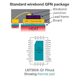
A typical package like a wire-bond quad flat no-lead (QFN) has a junction/die that usually connects to a thermal pad for heat dissipation (Fig. 1). The junction has bond wires to connect the junction to the pins. The bond wires are very thin and don’t conduct heat very well, resulting in most of the heat escaping from the thermal pad.
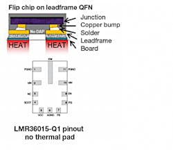
Flip-chip technology flips the chip/junction so that the copper bumps are upside down and soldered directly to the lead frame (Fig. 2). This results in reduced parasitic impedances from the pin to the junction, improving efficiency, size, switch ringing, and overall performance for a given specification. The flipped chip, however, prohibits the die from connecting directly to a thermal pad, as there’s no thermal pad on typical flip-chip devices.
Fortunately, the elimination of the bond wires facilitates paths of high thermal conductivity from the die, through the pins and into the board. This results in good thermal conduction between the die and the board, thus removing heat from the IC.
Using Pins to Optimize Heat Distribution
Power-supply designers can achieve very good thermal performance with flip-chip ICs by connecting and using flip-chip pins for heat distribution. Connecting the pins to large copper traces and polygon pours reduces the thermal resistance and pulls more heat out of the package.
The power-ground (PGND) pin is often used to extract heat from the IC. PGND also requires higher current capability; therefore, the copper bump connecting the junction to the PGND pin is typically larger than the copper bump of a signal pin. This larger copper bump allows for more heat to flow from the PGND pin(s). On the system side, PGND is electrically quiet, so a large copper surface area will not impact electromagnetic interference (EMI) levels—an important requirement in automotive systems.
You can use other pins for improved thermal performance, but take care not to increase the surface area of noisy nodes such as the switch node and the bootstrap pin. This can impact EMI performance and may cause violations of EMI test limits.
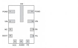
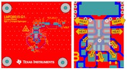
Let’s test these strategies using the LMR36015-Q1. The flip-chip buck converter is rated for 150°C and handles inputs to 60 V and can deliver up to 1.5 A (Fig. 3).
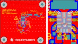
In a thermally optimized layout of the LMR36015-Q1 (Fig. 4), pins 1 and 11 are PGND pins connecting to a large ground plane, providing good heat distribution. The layout also uses thermal vias on the ground plane, harnessing the inner layers for even more heat distribution. Pin 6 is analog ground, which also has a large ground plane and thermal vias.
Pins 2 and 10 are the input voltage (VIN) pins, which like the PGND pins have large internal copper bumps for increased current capacity and improved thermal conductivity for better heat dissipation. The input voltage on a buck converter is inherently noisy, though, so watch the size of the VIN plane to avoid pushing EMI levels past acceptable limits. The switch node and bootstrap pin are noisy due to fast changes in voltage, so it’s important to keep those nodes as small as possible.
The LMR36015-Q1 board measures 2.2 × 2.3 inches (5.6 cm × 5.8 cm) and only has two layers. Typical boards are larger and contain four or more layers, and this increase in size and number of layers also exacerbates the thermal challenge. The thermally optimized layout enables the LMR36015-Q1 to operate at 12 VIN, 5 VOUT at a full load of 1.5 A, switching at 400 kHz with a temperature rise of only 28°C in a 22°C still-air environment. This layout also allows the 150°C-rated IC to operate in ambient temperatures as high as 115°C, which gives 10°C of margin above the 105°C ambient requirement that’s used in some of the harshest automotive environments.
Smaller-power ICs in flip-chip packages don’t necessarily result in poor thermal performance. When compared to wire-bond packages, it’s possible to achieve equivalent thermal performance by following the guidance presented in this article.
Sam Jaffe graduated with a joint Bachelors/Masters in Electrical Engineering from California Polytechnic State University in San Luis Obispo in June of 2016. He joined TI in August of 2016 and has worked as a Field Sales representative, an applications engineer in the high-voltage power group, and for the last two-and-a-half years, in the Wide VIN Buck Converters and Controllers group.
About the Author
Samuel Jaffe
Applications Engineer, Wide VIN Buck Converters and Controllers, Texas Instruments
Sam Jaffe graduated with a joint Bachelor’s/Master’s in Electrical Engineering from California Polytechnic State University in San Luis Obispo in June of 2016. He Joined TI in August of 2016 and has worked as a Field Sales representative, an applications engineer in the high-voltage power group, and the last two-and-a-half years in the Wide VIN Buck Converters and Controllers group.
