Half-Bridge Driver Features Floating Grounds, Resistor-Programmable Dead Time

Power devices such as N-channel MOSFETs count on a controllable, well-behaved driver to manage their critical on/off timing and other key attributes. The LTC7060 half-bridge driver developed by Analog Devices targets the needs of the half- and full-bridge converters used in automotive, industrial, and telecom power systems. It features easily programmable dead time and shoot-through protection, bolstered by a unique double floating-ground architecture for both the low- and high-side gate drivers.
This arrangement for driving dual N-channel MOSFETs makes the device’s outputs robust and less sensitive to ground noise. Meanwhile, the symmetric design allows the half-bridge output to be inverting or non-inverting with respect to the input logic. Its noise immunity tolerates ±10-V ground difference between input and output ground potentials.
In operation, the LTC7060 accepts a ground-referenced, low-voltage digital pulse-width-modulated (PWM) signal to drive two N-channel power MOSFETs in a half-bridge configuration (see figure). The gate of the low-side MOSFET is driven high or low, transitioning between the bottom-side driver voltage and the bottom-side ground voltage depending on the state of the PWM pin. Similarly, the gate of the high-side MOSFET is driven in a mode which is complementary to that of the low-side MOSFET, swinging between the top-side driver voltage and the top-side MOSFET driver return.
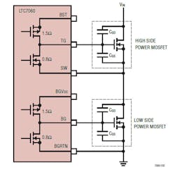
The 0.8-Ω pull-down and 1.5-Ω pull-up resistor capability supports delivering output currents with very short transition times to easily drive the large gate capacitances of high-voltage MOSFETs. Other features of this device include programmable dead time via an external resistor, as well as adaptive shoot-through protection to prevent current spikes and likely failure resulting from MOSFET cross-conduction.
The datasheet includes detailed tables as well graphs of key performance parameters such as rise and fall times versus floating supply voltage and versus load capacity. There are also graphs of dead time versus resistor value, temperature, and floating supply voltage, among others.
The LTC7060 operates from a 6- to 14-V supply rail and supports 4- to 14-V gate-driver voltages. Its 100-V maximum input voltage is independent of supply voltage and includes both undervoltage and overvoltage lockout detectors that monitor the supply rail. The IC comes in a thermally enhanced 12-lead MSOP package and is undergoing AEC-Q100 qualification. Pricing begins at $1.04 (1000 pieces); more information is available on the LTC7060 datasheet.
About the Author

Bill Schweber
Contributing Editor
Bill Schweber is an electronics engineer who has written three textbooks on electronic communications systems, as well as hundreds of technical articles, opinion columns, and product features. In past roles, he worked as a technical website manager for multiple topic-specific sites for EE Times, as well as both the Executive Editor and Analog Editor at EDN.
At Analog Devices Inc., Bill was in marketing communications (public relations). As a result, he has been on both sides of the technical PR function, presenting company products, stories, and messages to the media and also as the recipient of these.
Prior to the MarCom role at Analog, Bill was associate editor of their respected technical journal and worked in their product marketing and applications engineering groups. Before those roles, he was at Instron Corp., doing hands-on analog- and power-circuit design and systems integration for materials-testing machine controls.
Bill has an MSEE (Univ. of Mass) and BSEE (Columbia Univ.), is a Registered Professional Engineer, and holds an Advanced Class amateur radio license. He has also planned, written, and presented online courses on a variety of engineering topics, including MOSFET basics, ADC selection, and driving LEDs.
Comment About the Article
To join the conversation, and become an exclusive member of Electronic Design, create an account today!

Leaders relevant to this article: