Maximize Thermal Performance in Automotive DC-DC Converters
Download this article in PDF format.
A dc-dc converter is an electric circuit that converts a source of direct current (dc) from one voltage level to another by storing the input energy temporarily and then releasing that energy to the output at a different voltage. Converters protect electronic devices from power sources that are too strong or step up the level of the system input power to ensure it runs properly. The push to higher power density and the necessity for higher efficiency makes a modular dc-dc converter a demanding environment for power ICs, requiring designers to set new standards in thermal resistance and volumetric efficiency.
All dc-dc converters dissipate power in the form of heat. This heat must be managed properly so that the converter maintains operation within the recommended temperature limits to improve reliability and prevent premature failure. With power components coming in smaller and smaller surface-mount packages, it’s important to lessen the thermal-dissipation demands of these components. Unfortunately, as electronic parts get smaller, it becomes harder to secure the surface area in contact with air that’s necessary to achieve effective heat dissipation.
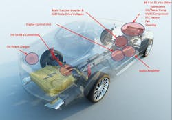
In particular, thermal management is critical in development of hybrid and electric vehicles since they contain multiple high-density power modules (Fig. 1). During operation, EV power electronics generate large amounts of heat (hundreds of watts per die), which leads to large heat flux at the die and package levels. What’s more, under-hood temperatures can climb to well above 150°C, depending on operating conditions.
Sponsored Resources:
Proper PCB Design
Without a thoughtful printed-circuit-board (PCB) layout to spread the heat, using smaller ICs in a design might result in a significant temperature rise. That’s especially concerning for automotive applications as thermal design must ensure that the junction temperature doesn’t exceed the rated temperature of power components (switching FETs), which are the main heat sources.
Automotive PMIC packages are now commonly equipped with an exposed pad (EP) for substrate thermal bonding so that even small electronic parts can effectively dissipate heat through the EP and PCB. Most heat generated by power ICs dissipates from the EP on the back of the package.
Utilizing a two-layer PCB for an automotive power supply design can provide significant system cost savings as compared to a larger four-layer approach. Regrettably, this tradeoff has traditionally resulted in decreased thermal performance.
When using a two-layer board, more care is required than using a multilayer board. Why? For starters, the multilayer circuit board often has a top trace layer on which the module is mounted and two buried copper (Cu) planes that are connected with vias to the top layer. This structure can have very high thermal conductivity (low thermal resistance), which allows heat to readily flow away from the module.
A two-layered board, however, has no inner Cu plane, so thermal resistance might be higher compared to a multilayer board. Furthermore, because both sides are typically used as wiring layers, it’s difficult to have a Cu plane. Even if a Cu plane is connected to the ground plane on the back of EP through vias, the ground plane will be divided by wiring.
Optimizing Flip-Chip IC Thermal Performance
One common small-size package is a flip-chip IC. With flip-chip technology, the ICs are installed face down in the package with electrical connections between the chip and substrate via conducting “bumps,” and the heated part of the IC faces the bottom of the package. Flip-chip technology has been used in consumer, industrial, and automotive power-supply solutions for years. An important advantage of flip-chip assembly is its compactness, which reduces size and weight compared to traditional wire-bonded packages. This size reduction, though, has made thermal mitigation more challenging for several reasons.
For one thing, usually there’s no thermal die-attach pad to dissipate heat. Consequently, layout optimization is needed to reduce IC temperature for flip-chip devices—also known as HotRod devices at Texas Instruments. These don’t have a thermal pad to provide a path with high thermal conductivity to let the heat escape and keep the IC cool.
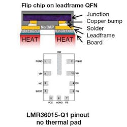
So, some layout modifications are required. Since there’s a low impedance connection between the die and the package, it provides a path for heat to flow out through each pin of the IC. As an example, let’s look at the TI LMR36015-Q1 flip-chip buck converter. The LMR36015-Q1 is in a HotRod package that enables low EMI, higher efficiency, and the smallest package-to-die ratio. The device requires few external components. Figure 2 shows the pinout of the LMR36015-Q1.
A thermally optimized layout allows the flip-chip buck converter to be rated for 150°C, handle inputs to 60 V, and deliver up to 1.5 A. It also able to operate in ambient temperatures as high as 115°C, giving it sufficient margin above the 105°C ambient requirement that exists in harsh automotive environments.
No thermal pad means most of the heat will escape through the pins of the IC and into the board. Flip-chip devices have a direct connection from the die to the pins to increase thermal conductivity. And some of the pins are elongated to get more heat out.
Connecting the pins to large copper traces and polygon pours (multi-sided areas of copper) reduces the thermal resistance and pulls more heat out of the package. Power-ground (PGND) pins (pins 1 and 11 in Fig. 2) connecting to a large ground plane provide good heat distribution and can be used to extract heat from the IC.
Other pins also can be used for improved thermal performance. For example, Pin 6 is analog ground (AGND), which also has a large ground plane and thermal vias. Pins 2 and 10 are the input voltage (VIN) pins, which like the PGND pins, have large internal copper bumps for increased current capacity and improved thermal conductivity for better heat dissipation.
Enhanced HotRod QFN Packages
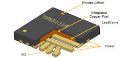
TI’s quad flat no-leads (QFN) HotRod is a thermally enhanced plastic package that uses copper leadframe technology (Fig. 3). It eliminates power-device wire bonds by attaching the power device and/or die directly to the leadframe. This construction results in cost-effective packaging that improves electrical and thermal performance over traditional leaded packages. By eliminating the wire-bond connection between the die and the leadframe, the HotRod QFN also minimizes the package parasitic inductance and resistance.
TI’s Enhanced HotRod QFN package leverages the noise improvements of the flip-chip-on-leadframe (FCOL) package and the thermal advantages of the standard QFN package. By employing the standard QFN package technology, the enhanced HotRod QFN package uses a center PowerPad IC package to dissipate heat. In the LM60440 synchronous step-down converter, 4 A is achieved at an ambient temperature of 85°C. TI’s LM60430-Q1 dc-dc converter also offers Enhanced HotRod QFN package technology.
Conclusion
For automotive applications, dc-dc converters are evaluated on key performance metrics like efficiency, size, noise, and thermal performance. Thermal countermeasures are necessary when dealing with the board’s heat dissipation. The package technology used can influence the performance of this metric, and the package technology for best thermal performance depends on the PCB design rules used in the application.
This article discussed the strategies that can be implemented in the layout to optimize thermal performance. It also demonstrated that even though flip-chip quad flat no-leads (in Texas instruments parlance, “HotRod”) packaging typically lacks the large thermal pad present on the bottom of standard QFN packages, it can maximize thermal performance. That’s because the low-impedance connections between the die and the package pins provide a path for heat to conduct out of IC pins. Furthermore, by employing standard QFN package technology, the TI Enhanced HotRod QFN package, using a center PowerPad IC package, is an effective means to dissipate heat.
Sponsored Resources:
About the Author
Murray Slovick
Contributing Editor
Voice Your Opinion!
To join the conversation, and become an exclusive member of Electronic Design, create an account today!

Leaders relevant to this article:


