Compact 300-mA LDOs Target High-Performance ADAS Sensors

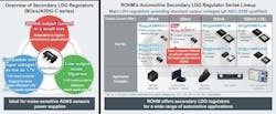
In recent years, safety requirements in the automotive sector have expanded as technological innovations in accident prevention and autonomous driving continue to progress. In line with this, sensors and cameras installed in advanced driver-assistance systems (ADAS) now need power-supply ICs that deliver larger currents in a smaller package size.
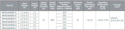
To meet those demands, ROHM Semiconductor introduced the new BUxxJA3DG-C series of automotive-grade low-dropout (LDO) regulator ICs (BU12JA3DG-C, BU15JA3DG-C, BU18JA3DG-C, BU25JA3DG-C, BU30JA3DG-C, and BU33JA3DG-C). These linear regulators are designed as low current consumption products for power supplies.
LDO regulators are a type of power-supply IC that converts between two different dc voltage levels. It falls under the category of linear regulator (where the input/output voltages operate linearly) characterized by a small input-output voltage difference. Compared to dc-dc converter ICs (switching regulators), LDOs feature a simpler circuit configuration and lower noise.
These parts are designed for up to 6.5 V as an absolute maximum voltage and operate to 300-mA output current with low current consumption (37µA typ). The parts can regulate the output with an accuracy said to be ±2%.
Thanks to the low input supply voltage, the LDO can be used in 1.8-V power-supply systems to provide low output voltages at a higher efficiency. Furthermore, the output voltage noise is reduced to just 55 μVRMS, which is about 40% lower than similar 3.3-V low-noise LDO regulators. As a result, the BUxxJA3DG-C series provides a quieter power supply, along with greater power savings and miniaturization in automotive applications.
The devices feature integrated overcurrent protection to guard them from damage caused by short-circuiting or an overload. These products also integrate thermal-shutdown protection to avoid damage from overheating. A logical "HIGH" at the EN pin turns on the device, and on the other side, the devices are controlled to disable via a logical "LOW" input to the EN pin.
The new BUxxJA3DG-C series meets the basic requirements for LDOs used in the secondary power supplies of automotive systems (i.e., compact size, compatibility with standard output voltages). In addition, despite their small package size (2.9 × 2.8 mm), they support output currents of up to 300 mA while covering an input voltage range from 1.7 to 6 V.
The LDO series also supports 125°C operation, qualification under the AEC-Q100 automotive reliability standard, and output voltages for automotive secondary LDO regulators. By way of review, in an automotive power supply, the side in charge of first-stage conversion from a power source, such as a battery, is called the primary. Similarly, the side responsible for second-stage conversion is called the secondary. Power-supply ICs for primary applications are required to support high input voltages, while secondary power-supply ICs operate in the low input/output regime.
Output noise is reduced by 40% over general products (e.g., 55 μVRMS for BU33JA3DG-C), reducing the effect on minute electrical signals. Thus, the parts well-suited for power supplies in compact, high-performance automotive applications where noise is a concern. The low-noise design also improves system reliability
Passives
If the battery is placed far from the regulator, or the impedance of the input side is high, higher capacitance is required for the input pin capacitor to prevent a voltage drop at the input line. The input capacitor and its capacitance should be selected depending on the line impedance, which is between the input pin and the smoothing filter circuit of the power supply.
Therefore, an appropriate capacitance value that’s selected by the consideration of the input impedance is different for each application. Generally, the capacitor with a capacitance value of 0.1 µF (min) with good high-frequency characteristic is recommended for this regulator.
The output pin capacitor is mandatory for the regulator to realize stable operation. The output capacitor with a capacitance value ≥ 0.47 µF (min) and ESR up to 1 Ω (max) is required between the output pin and the GND pin. Appropriately selected capacitance value and ESR for the output capacitor can improve the regulator’s transient behavior.
Application examples include automotive powertrain, body ECU, infotainment clusters, head-up displays, ADAS sensors, cameras, and radar and secondary power supplies for noise-sensitive automotive applications. Pricing is $1.00/unit (samples, excluding tax). The series is available now (in mass production) through online distributors Digi-Key, Farnell, and Mouser.
About the Author
Murray Slovick
Contributing Editor
Comment About the Article
To join the conversation, and become an exclusive member of Electronic Design, create an account today!

Leaders relevant to this article: