650-V Power MOSFET in QDPAK Targets Fast EV Charging

In electric vehicles, the battery capacity and energy efficiency of components must be optimized to achieve desired driving ranges. By reducing charging times and vehicle weight, engineers also can increase design flexibility and cut the total cost of ownership of the vehicle.
Other obvious EV development targets include efficient power conversion in 400- and 800-V systems, power density, reliability, and bidirectional power flow to enable future use cases like vehicle-to-load (V2L), vehicle-to-home (V2H), and vehicle-to-grid (V2G). Similarly, cost-effective HV-LV DC-DC conversion solutions for EV architectures must be designed to support a wide range of efficient conversion topologies where compact designs, high power density with minimum space, bidirectional power flow, and wide voltage ranges are key application design requirements.
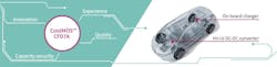
Targeting these goals, Infineon said the latest silicon-based 650-V CoolMOS SJ power MOSFETs in its expanded CFD7A lineup are specifically optimized to meet the requirements of EV applications such as on-board chargers, HV-LV DC-DC converters, and auxiliary power supplies.
Enter the QDPAK
The 650-V CFD7A portfolio introduces the QDPAK package. This package family is designed to provide equivalent thermal capabilities with improved electrical performance over well-known TO-247 devices, thus enabling more efficient energy utilization.
This addition complements the existing CoolMOS CFD7A series, offering top- and bottom-side cooled packages. The QDPAK TSC (top-side cooled) enables designers to achieve higher power densities and optimal PCB space utilization.
To obtain reliable operation in high-voltage applications, the CFD7A reduces parasitic source inductance as well as minimizes electromagnetic interference (EMI), ensuring clear signals and consistent performance. Its Kelvin source pin improves precision for current sensing, bringing accurate measurements even in challenging conditions.
With a creepage distance said to be suitable for high voltage applications, in addition to high-current capability and high power dissipation (Ptot) of up to 694 W at 25°C, the part is a versatile device for a wide range of high-voltage applications.
Thermal Benefits
This introduction also highlights what many in the industry have long understood—the importance of adequate cooling. According to Infineon, new system designs using the 650-V CoolMOS CFD7A in QDPAK top-side cooling (TSC) will maximize the use of PCB space, double power density, and enhance thermal management via substrate thermal decoupling.
That last item is important since the amount of heat generated by each chip leads to thermal coupling among devices, which in turn increases in temperature. Here the approach to thermal management simplifies assembly, eliminates board stacking, and reduces the need for connectors, also thereby lowering system costs. Infineon said that the power switch reduces thermal resistance by up to 35%, providing high power dissipation that outperforms standard cooling solutions.
Infineon’s approach overcomes the thermal limitations of bottom-side cooled SMD designs using FR4 PCBs, boosting system performance. The optimized power loop design locates drivers near the power switch, improving reliability by reducing stray inductance and chip temperatures. Overall, these features contribute to an efficient system that’s well-suited for modern power needs.
As announced in February 2023, the QDPAK TSC package has been registered as a JEDEC standard for high-power applications, helping to establish a broad adoption of TSC in new designs with one standard package design and footprint. To further accelerate this transition, Infineon will also release additional automotive-qualified devices in QDPAK TSC for onboard chargers and DC-DC converters in 2024, such as 750- and 1200-V CoolSiC devices.
In February of this year, Ralf Otremba, Lead Principal Engineer for High Voltage Packaging, Infineon noted, “As a solutions provider, Infineon continues to influence the semiconductor industry through innovative packaging technologies and manufacturing processes.
“Our advanced top-side cooled packages bring significant advantages to the device and system levels to fulfill the challenging demands of cutting-edge high-power designs. Package outline standardization will help ease one of the main design concerns of OEMs for high-voltage applications by securing pin-to-pin compatibility across vendors.”
With the CoolMOS CFD7A, higher switching frequencies can be achieved at gate-loss levels comparable to former generations. Furthermore, this combination enables the CFD7A decrease system weight and space, resulting in more compact designs.
Infineon said the CoolMOS CFD7A family is manufactured on a highly automated 300-mm production line, which contributes to efforts to reach the zero-defect target in mass production while fulfilling a growing market demand.
The 650-V CoolMOS CFD7A in the QDPAK package comes in top-side cooled and bottom-side cooled versions, both of which are available now.
About the Author
Murray Slovick
Contributing Editor
Comment About the Article
To join the conversation, and become an exclusive member of Electronic Design, create an account today!

Leaders relevant to this article: