How Does Lockstep Architecture Enhance MCU Performance?
What you'll learn:
- Understand how lockstep architecture improves fault detection, redundancy, and real-time reliability in safety-critical microcontroller systems.
- Explore the applications of lockstep processors in automotive, aerospace, and industrial environments, including their role in meeting ISO 26262 and ASIL-D safety standards.

In the dynamic world of microcontroller (MCU) technology, ensuring reliable and robust performance is crucial, particularly for critical applications such as automotive systems. On that front, lockstep architecture has become a pivotal technology that boosts both the performance and reliability of MCUs.
Lockstep architecture is vital in safety-critical systems where failure may result in significant consequences. By running duplicate systems in parallel and comparing outputs, lockstep processors can quickly detect and respond to faults, helping to ensure operational integrity and system safety. This makes lockstep architectures indispensable in sectors that demand high reliability, such as automotive, aerospace, and industrial control systems.
This article explores the fundamentals of lockstep architecture and its significance in enhancing MCU capabilities. Lockstep technology’s broader implications and applications in hardware chips are also addressed, especially within the automotive industry.
What is Lockstep?
Lockstep architecture refers to a MCU/processor design methodology in which two or more redundant cores execute the exact instructions simultaneously. This synchronous execution enables the system to detect and correct errors by comparing the outputs of the redundant cores. If a discrepancy is detected, it indicates a fault in one of the cores, prompting corrective measures to ensure the system continues to function correctly.
Lockstep architecture is vital in applications where safety and reliability are critical. It provides an added layer of fault tolerance by ensuring that the other core can provide the correct output even if one core fails or produces incorrect results due to a transient fault or hardware failure. This makes lockstep preferred in systems requiring high functional-safety levels.
The primary advantage of lockstep architecture is its ability to detect errors in real-time without impacting the system’s performance. Unlike traditional error-detection methods that require additional error checking and correction cycles, lockstep architecture performs these tasks concurrently with the main computation. This parallel execution helps maintain high system performance while ensuring robustness and reliability.
Lockstep Processors for Safety-Critical Systems
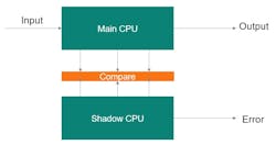
Lockstep architecture boosts the safety and reliability of microcontrollers used in safety-critical systems, such as those found in automotive applications. It involves dual or multiple cores that operate in parallel, executing the exact instructions simultaneously (Fig. 1). This redundancy allows for immediate fault detection, as any discrepancies between the cores’ outputs can be swiftly identified and addressed.
The fundamental advantage of lockstep processors lies in their fault-detection and error-correction mechanisms. These are vital in automotive-grade processors where reliability is paramount. The architecture ensures that in the event of a fault in one core, the system continues to operate safely by relying on the output from the synchronized core. Such a capability helps meet stringent safety standards, such as ISO 26262, which governs the functional safety of electrical and electronic systems within road vehicles.
For example, Infineon’s AURIX TC4 microcontroller utilizes its unique “Diverse Lockstep” architecture technology to achieve high reliability and performance. This underpins the ability to demanding applications like advanced driver-assistance systems (ADAS) and engine control units (ECUs).
The AURIX TC4 is designed to comply with ASIL-D standards, the highest safety integrity level under ISO 26262. It integrates dual-core lockstep execution that supports real-time fault detection without impacting system performance.
>>Download the PDF of this article

Further technical sophistication in lockstep processors includes the integration of error-detection hardware mechanisms, which bolster the processor’s ability to handle unexpected operational anomalies. Software programming also plays a pivotal role, particularly in configuring the lockstep mechanism to efficiently manage parallel execution and error-handling processes.
In multicore configurations, such as those supporting up to six cores, lockstep execution can extend to multiple pairs, enhancing computational power and fault tolerance. This approach ensures high levels of safety and reliability and reduces development costs and efforts by simplifying the system design and verification processes.
Other Applications of Lockstep in Hardware Chips and Automotive
Lockstep architecture extends beyond traditional applications to deliver high reliability and safety. For example, lockstep is essential for the flight control systems in avionics to ensure accuracy and immediate fault correction in its control algorithms. Network processors employ lockstep in telecommunications (see “Hacking Lockstep Doubles the Fun” below) to maintain data integrity and ensure continuous service by detecting and correcting errors in real-time.
In the automotive industry, lockstep architecture is integral across multiple applications. Vehicles today incorporate numerous ECUs managing functions from engine performance to safety operations like braking and airbag deployment. Lockstep architecture ensures these ECUs function reliably, swiftly detecting and responding to faults to maintain safety.
In autonomous vehicles, lockstep is employed in CPUs that process sensor data and execute real-time driving decisions. This redundant execution makes sure that faults in data processing are immediately identified, allowing for immediate corrective actions to sustain safe operations.
ADAS like lane-keeping assistance and collision avoidance also rely on lockstep for accurate and reliable data processing, thus enhancing vehicle safety. In certain lockstep applications, two processors run in parallel, executing identical instructions simultaneously to enhance reliability and fault tolerance. If one processor fails, the standby processor seamlessly takes over real-time processing until the issue is resolved (Fig. 2).
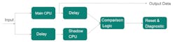
Synchronization establishes that both processors reach the same state after executing each instruction, achieved through hardware signals, clock signals, or software-based mechanisms. The standby processor detects the fault, assumes control, and maintains continuity of operations. This redundancy is vital in safety-critical systems like automotive control units and aerospace applications that require uninterrupted real-time processing for overall system reliability and safety.
Furthermore, considering the resilience of ASIL D-certified microcontrollers against fault injection attacks, lockstep architecture plays a pivotal role. It provides a robust defense mechanism against hardware-centered attacks and significant threats to automotive security. By integrating redundant processing and continuous cross-checking, lockstep architecture can effectively identify and mitigate discrepancies caused by such attacks, thereby enhancing the security and resilience of automotive systems against malicious exploits.
Conclusion
Lockstep architecture’s real-time error-detection and correction capacity — without affecting system performance and redundancy — makes it indispensable in industries where safety and reliability are critical. This includes industries such as automotive, aviation, and telecommunications.
The technology ensures operational integrity and enhances system resilience against random faults and security threats, particularly in automotive applications where it mitigates risks associated with hardware-centered attacks. Its use case in parallel processing to enhance reliability enhances vehicle safety.
Therefore, it’s important to use a device that employs the capabilities of lockstep architecture in meeting high safety and performance standards. Moreover, such a device should serve the broader application of this technology as it continues to evolve, promising even more significant advances in the safety and security of complex electronic systems.
References
https://ieeexplore.ieee.org/document/9516749/
https://ieeexplore.ieee.org/document/8574582/
https://ieeexplore.ieee.org/document/10187275/
Hacking Lockstep Doubles the Fun
—By Andy Turudic, Electronic Design Technology Editor
Back in my senior year in university, we went on a field trip, touring the Pickering Nuclear Power Plant (we got to go inside the CANDU Reactor Number 3 building, which was under construction, as well as to see the Cherenkov radiation in the spent fuel bay’s pool) and Canada’s flagship technology manufacturer, Northern Telecom (Nortel). I was planning to go into digital automotive instrumentation design at that time, but one look at that Nortel digital central office system on that field trip and I fell in love and found my calling. Your loss, Detroit.
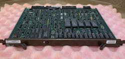
After graduation, I started out in Nortel’s Test Engineering group for the DMS-100 Digital Switching System (Fig. 3), primarily working on testing its “NT40” central processor core’s I/O subsystem: circuit packs for the I/O controller and control CPs for 9-track mag tape, ASCII terminals, and, eventually the 14-in. Winchester hard drive (Fig. 4). I also worked on its high-accuracy central clock system.
The central processor was a custom instruction set, Harvard architecture, stack-based, 16-bit machine comprised of around 500 TTL chips across two, redundant, lockstepped cores. Each had its own rack with DRAM in a couple of shelves of cards below, and a messaging and clock system in the shelf above, the CPU shelf. Power supplies in each shelf were redundant and hot-pluggable, and all of the circuit packs had advance ground pins, which also enabled hot plugging.
The eventual replacement of Schottky TTL devices with FAST (Fairchild Advanced Schottky TTL) logic in critical paths bumped the processor speed up to a blazing 40 MHz. While this may seem slow by today’s standards, the NT40 was capable of switching the calls for close to 100,000 phone lines in a fully digital system while running a high-level, internal, procedure-based language: “Protel.”
Having this machine boot up in firmware was a geek’s delight, as each processor was put into a tight loop, with one of the machines executing an extra machine instruction cycle per loop. The program bus address (Harvard machines have separate program and data storage systems) would slip one machine cycle for each loop completion, with the program address registers being monitored by a “match registers” (Simran's Fig. 1) to determine when the machines were both cycle-synchronized. At this point, they’d kick out of the loop and subsequently execute code in complete synchronization, ad infinitum, with one processor designated as “active” and the second on “standby.”
Should a program address mismatch occur, the machine would declare a “dropped sync” condition (Simran's Fig. 2). It would designate one of the two processors as “active” depending on which side had a fault (usually a memory parity error), without skipping a beat as far as high-level code was concerned.
The entire central office of Nortel’s $2M (1980 money, today $8M, though the NT40 could now fit easily on an FPGA) DMS-100 system, was guaranteed to have a down time of less than two hours in 40 years. This is in large part due to the lockstepped NT40 processor architecture and other redundancies that enabled maintenance of live, running machines.
There’s nothing more eerie than being in a live central office, one in which people are talking within the machine's digital timeswitching memory circuits and who need to be able to dial a 911 (emergency services) at any moment, and pulling the redundant-provisioned master telecom network clock circuit pack out to modify its power supply. Don't ask how I know this.
A problem arose when our software developers would run regression and validation on builds in the “lab,” as these could only be performed on actual, running, DMS-100 machines. At $2M each, we quickly realized that lockstep was completely unnecessary in a captive development lab environment, thereby doubling the number of “active” machines capable of running validation and regression tests.
I was given the task of designing circuit boards and building a small bit of hardware that plugged into the backplane’s rear pins that would break the lockstep and fake signals. It would make it look like the “mate” processor was happy and still in sync, despite running a completely different software load. As unsync’d as it could get.
The “Splitter” became a high-demand bit of kit worldwide. As a freshly minted engineer, I got to travel to our satellite development locations to install Splitters, including Calgary, Dallas, Research Triangle Park (RTP) N.C., and the UK, doubling our productivity at each site. It was the relationships we cultivated from my visit in RTP from hacking their lockstepped NT40s, and my circuit design and manufacturability acceptance experience, that had RTP subsequently invite me to join their hardware design team a few years later in North Carolina.
So, embrace lockstep processors and you’ll work on great projects and go places as an engineer. Places like Embedded World in Germany. -andyT
Andy's Nonlinearities blog arrives the first and third Monday Tuesday of every month. To make sure you don't miss the latest edition, new articles, or breaking news coverage, please subscribe to our Electronic Design Today newsletter. Please also subscribe to Andy’s Automotive Electronics bi-weekly newsletter.
>>Download the PDF of this article
About the Author
Simran Khokha
Product Manager, Infineon Technologies
Simran Khokha is a product manager at Infineon, Germany. Simran has dual MSc degrees from NTU, Singapore, and TUM, Germany, in electrical engineering. She has half a decade of experience in consumer product tech companies including AMD, Realtek, and STMicroelectronics, serving product development and design roles in Singapore and now in product management and marketing in Europe. She has been focused across a wide range of segments including automotive, IoT, and consumer electronics. Simran has previously worked in designing first-of-their-kind SoCs used for AI/ML, self-driving cars, and future applications.

Andy Turudic
Technology Editor, Electronic Design
Andy Turudic is a Technology Editor for Electronic Design Magazine, primarily covering Analog and Mixed-Signal circuits and devices and also is Editor of ED's bi-weekly Automotive Electronics newsletter.
He holds a Bachelor's in EE from the University of Windsor (Ontario Canada) and has been involved in electronics, semiconductors, and gearhead stuff, for a bit over a half century. Andy also enjoys teaching his engineerlings at Portland Community College as a part-time professor in their EET program.
"AndyT" brings his multidisciplinary engineering experience from companies that include National Semiconductor (now Texas Instruments), Altera (Intel), Agere, Zarlink, TriQuint,(now Qorvo), SW Bell (managing a research team at Bellcore, Bell Labs and Rockwell Science Center), Bell-Northern Research, and Northern Telecom.
After hours, when he's not working on the latest invention to add to his portfolio of 16 issued US patents, or on his DARPA Challenge drone entry, he's lending advice and experience to the electric vehicle conversion community from his mountain lair in the Pacific Northwet[sic].
AndyT's engineering blog, "Nonlinearities," publishes the 1st and 3rd Tuesday of each month. Andy's OpEd may appear at other times, with fair warning given by the Vu meter pic. His cartoon series, "Inventors", appears each week in Electronic Design Weekly.
Comment About the Article
To join the conversation, and become an exclusive member of Electronic Design, create an account today!

Leaders relevant to this article: