Veeco touts 100 automated MBE systems installed worldwide

Plainview, NY. Veeco Instruments Inc. today announced it has completed installation of its 100th automated Molecular Beam Epitaxy (MBE) system. The installation of Veeco’s GEN10 MBE System last month at Silanna Semiconductor PTY Ltd. in Australia marks this company milestone. The company also operates a Veeco Dual GEN200 MBE System for production of advanced nitride compound semiconductor devices including ultraviolet LEDs (UV-LEDs).
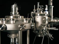
Silanna is using the GEN10 system for advanced oxide research and development (R&D) for optoelectronic devices. The GEN10 is built upon almost 20 years of cumulative automation knowledge and derived from the company’s production MBE systems. Adopted by numerous leading corporations, institutions, and universities for all major MBE applications, many customers choose the GEN10 because of its flexibility, which allows them to configure the system based on their application. This gives customers optimal performance with any material set, including those related to III-V group elements, oxides, and nitrides.
“Silanna has achieved remarkable results on its previous MBE systems, and Veeco is honored to celebrate this momentous accomplishment in our company history in partnership with Dr. Atanackovic and the Silanna team,” said Gerry Blumenstock, vice president and general manager, Veeco MBE Products. “As our customers explore novel materials and new applications, they can rely on Veeco to deliver innovative MBE systems, sources, and components for use in complex R&D, as well as high-volume production environments.”
MBE is a highly precise thin-film deposition method for creating crystals by building up orderly layers of molecules on top of a substrate. MBE is used in industrial production processes as well as nanotechnology research in high-growth advanced computing, optics, and photonics applications, to name a few. With over 600 systems shipped worldwide, Veeco said it provides the industry’s broadest portfolio of proven, reliable MBE systems, sources and components to serve a wide variety of markets and applications.
The Silanna Group was founded in 2006 and is headquartered in Brisbane, Australia, with operations and design centers in Sydney, Australia; San Diego, California; Raleigh, North Carolina; and Singapore. The group’s charter is to develop and productize advanced technologies. Silanna’s current technology portfolio includes advanced silicon and compound semiconductor technologies. Learn more at https://www.silanna.com/.
To learn more about Veeco’s equipment and services, visit www.veeco.com.
About the Author
RN (editor)
Comment About the Article
To join the conversation, and become an exclusive member of Electronic Design, create an account today!

Leaders relevant to this article: