Applying MOSFETs to Today’s Power-Switching Designs
Download this article in .PDF format
In the wake of gallium-nitride (GaN) transistor introductions, a number of semiconductor makers have begun to reassess the role played by conventional MOSFETs. The introduction of GaN devices doesn’t automatically obsolete the legacy MOSFETs, but the prospect of improving power-supply efficiencies and reducing their form factors is stimulating the imagination of analog engineers. In advance of what some are calling “The GaN Revolution,” it makes sense to review what legacy part types are available, and what you can do with them.
Until fairly recently, the power transistor world was roughly divided between two types of power transistors: MOSFET switches and bipolar junction transistors (BJTs). MOSFET switches, whose rapid turn-on/turn-off capability and low on-resistance (RDS(on)) make them useful for power switching circuits, remains the dominant transistor type. There are roughly 40 billion MOSFETs shipped each year.
MOSFETs conduct electrical current on one direction (or, rather, conduct most efficiently in one direction), but their ability to turn on and turn off rapidly in response to a voltage change at their inputs (gate voltage) makes them useful as pulse generators. The best known power switching circuits are switching power supplies, but MOSFETs are also widely used for pulsed (dc) motor drives and Class D audio amplifiers.
Bipolars, IGBTs
Unlike power MOSFETs, whose turn-on/turn-off behavior is extremely rapid and (ideally) linear, bipolar transistors will generate “soft edges,” more closely resembling sine waves rather than square waves. They respond to current changes at their inputs, which makes them useful for driving relatively slow-changing inductive loads—motors, commodity power supplies, and audio speakers. Between 7 and 8 billion bipolar power transistors are used each year.
To get bipolar transistors to behave like amplifiers, you have to further soften their switching behavior. You need to bias the transistors in such a way that forces them to hang in a linear conduction region—never fully on and never fully off, but somewhere in between. While they are good at driving inductive loads, without the low RDS(on) of MOSFETs, they can get very hot.
A third type of transistor, the insulated-gate bipolar transistor (IGBT) is effectively a bipolar transistor with built-in gate drivers. It enables a somewhat faster turn-on/turn-off behavior for bipolar devices, though not as fast as MOSFETs. The special advantage of IGBTs is their ability to handle high voltages (in excess of 600 V) and currents, making IGBTs a favorite for industrial motor-drive applications in factory automation (where they drive conveyer belts and robot arms) and in automobiles (where they drive things like the moon roof and side-view mirror). About 1.5 to 2.5 billion IGBTs are shipped each year.
Characterizing Behavior
While power transistors are readily available with a wide range of voltage and current ratings, packaging, and manufacturers applications support, the inherit behaviors of bipolar transistors, MOSFETs, and IGBTs help define their application requirements. Because they’re also cheap in high volume (e.g., 12 to 15 cents each), 100-V bipolar transistors are routinely used, for example, to generate the ±40-V rails in audio power amplifiers. (Some suppliers include self-biasing mechanisms for audio BJTs.)
Meanwhile, the 600-V IGBTs find homes in motor drives, such as household appliances (washing machines and dryers), which interface with 220-V ac house lines. Switching power supplies are by far the most dominant applications for power MOSFETs. Here, what’s called a “low-voltage MOSFET”—25, 30, or 40 V—is used to generate the 5- or 12-V power rails employed in compute servers and communications switching stations.
While this may change, engineers have a tendency to over-specify voltage and current requirements. You’ll notice the IGBT that connects a washing machine to a 220-V line is rated for 600 or 650 V; the power train, a computer-server-card module supporting 5.0- or 3.3-V logic, starts with a 30-V MOSFET. And 100- or 200-V bipolar transistors are used to drive stereo loudspeakers.
The over-specification ensures power will always be available to the systems we’re powering. However, it also provides protection against sudden voltage spikes and current surges. (The automotive environment is particularly prone to transients, and 400-V-rated parts are specified to cope with 150-V load dumps.)
What may prevent engineers from over-specifying, eventually, is an ongoing smoothing, filtering, regulation and pre-regulation of the entire power-transmission chain. This affects compute-server architectures, for example, where suppliers like IBM and NTT DOCOMO advocate 385 V dc as the distribution voltage within a megawatt data center (and 48 V as the intermediate voltage within racks and cabinets). This would allow designers to reduce the margins with which they specify power components (a smaller, cheaper 60-V part, for example, in slots previously served by 100 V). In the meantime, engineers should pay attention to the “safe operating areas” (SOAs) specified in the transistors they hope to use.
Use the SOA
Switching-power-supply designers should pay attention to the SOA of the transistor they intend to use. The SOA is defined as the voltage and current conditions over which the device can be expected to operate without damaging itself.
The SOA is usually depicted as graph on the manufacturer’s datasheet. The current, in terms of amperes, is shown on the Y axis of an X-Y plot. The maximum drain-to-source voltage for a MOSFET (or the emitter-to-collector voltage for a bipolar junction transistor) is shown on the X axis. The curve typically resembles a “ski slope,” with the allowable current dropping off steeply with increasing voltage.
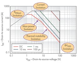
Since MOSFETs are typically used to generate pulse trains, some transistor vendors will depict SOA for the duration of the pulses (in milliseconds). If the transistor is left on (conducting dc), the maximum allowable current trails off faster than if the current is pulsed at 1-ms intervals, or at 10 ms. Pulsing the transistor at 100-µs intervals (equivalent to a 100-kHz switching speed) generates the largest SOA (Fig. 1). Thus, the SOA of any transistor will vary with its duty cycle, the ratio of its time “on” to its time “off.”
High- and Low-Side Switching
When selecting transistors, it may be advisable to pay attenton to how the MOSFETs are configured in a power-supply circuit. Specifically, determine whether the inductive (resistive) circuit load is connected between the MOSFET’s drain and the positive supply rail—a configuration called low-side switching—or whether the load is connected between the transistor’s source and ground—referred to as high-side switching.
The high- and low-side transistors don’t always behave in unison. While the high-side driver will do more work than the low-side driver, you don’t want it to latch to the positive rail. Similarly, you want the low-side driver to crash into ground. Thus, high- and low-side drivers will be specified differently.
In a low-side switch configuration, the source terminal of the n-channel FET is connected to ground; the drain connects to an inductive load, whose other terminal is connected to the positive supply rail. Any (positive) gate charge on the transistor turns it on and pulls current through the load. In the low-side configuration, it’s the gate threshhold voltage—3-V CMOS or 5-V logic level—that controls the behavoir of the switch.
In a high-side configuration, the drain of the MOSFET is connected to the positive supply rail, and the transistor’s source is connected to the load whose other terminal is connected to ground. In this configuration, the n-channel transistor’s gate must produce a voltage equal to the voltage across the load (almost equivalent to the supply voltage)—plus the gate threshhold voltage (3 V)—just to get the switch to turn on.
Channeling P- and N-Channels
It’s possible to make a simple high-side switch from P-channel MOSFETs. Using a negative voltage to get the P-channel MOSFET to turn “on” affects the threshold control. That is, getting the transistor to “conduct current” and letting it come up to the supply rail to turn it “off.”
But P-channel transistors are difficult-to-make devices, which will cost more than conventional N-channel FETs, and may need a negative gate voltage (or at least an attachment to ground) just to get it to turn on. This supports battery power for portables, but doesn’t readily lend itself well to switching-power-supply designs.
One solution is to combine N- and P-channel transistors in a totem-pole configuration in which they pull current in a “push-pull” configuration. Here, a high-side P-channel MOSFET and a low-side N-channel MOSFET have their drains tied together while their input gates are stimulated synchronously to affect a single high-current switch. During switching, designers will need to monitor crossover currents that may occur if the gate drive forces both MOSFETs to turn on simultaneously.
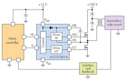
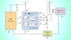
As an alternative to not-quite-matching P-channel and N-channel MOSFETs, designers can use gate-driver ICs that power high- and low-side MOSFETs (both N-channel devices) in a push-pull configuration. Both transistors can be switched on and off from one IC (Fig. 2).
As a final note, the relationship between the RDS(on) of the transistor under load and the swtiching behaviors of the MOSFET is not entirely positive (though low RDS(on) is generally the first MOSFET spec manufacturers and foundries will cite). The load RDS(on) number contributes to the efficiency of the FET—the lower the RDS(on),the smaller the heat disipation. However, this does increase transistor switching speed. The low RDS(on) tends to lengthen gate dimensions (adds capacitance) and makes them difficult to drive.
Looking for parts? Go to SourceESB.
About the Author
Comment About the Article
To join the conversation, and become an exclusive member of Electronic Design, create an account today!

Leaders relevant to this article: