One-Step Process Applies Graphene On Photonic, Electronic Materials
Researchers from the National University of Singapore (NUS), led by Professor Loh Kian Ping, who heads the Department of Chemistry at the NUS Faculty of Science, has successfully developed an innovative one-step method to grow and transfer high-quality graphene on silicon and other stiff substrates, opening up opportunities for graphene to be used in high-value applications that are currently not technologically feasible.
This breakthrough, inspired by how beetles and tree frogs keep their feet attached to submerged leaves, is the first published technique that accomplishes both the growth and transfer steps of graphene on a silicon wafer. This technique enables the technological application of graphene in photonics and electronics, for devices such as optoelectronic modulators, transistors, on-chip biosensors and tunneling barriers.
The innovation was first published online in prestigious scientific journal Nature on 11 December 2013.
Graphene has attracted a lot of attention in recent years because of its outstanding electronic, optical and mechanical properties, as well as its use as transparent conductive films for touch screen panels of electrodes. However, the production of high quality wafer-scale graphene films is beset by many challenges, among which is the absence of a technique to grow and transfer graphene with minimal defects for use in semiconductor industries.
Said Prof Loh, who is also a Principal Investigator with the Graphene Research Centre at NUS Faculty of Science, “Although there are many potential applications for flexible graphene, it must be remembered that to date, most semiconductors operate on “stiff” substrates such as silicon and quartz.”
“The direct growth of graphene film on silicon wafer is useful for enabling multiple optoelectronic applications, but current research efforts remain grounded at the proof-of-concept stage. A transfer method serving this market segment is definitely needed, and has been neglected in the hype for flexible devices,” Prof Loh added.
Drawing Inspiration From Beetles, Tree Frogs
To address the current technological gap, the NUS team led by Prof Loh drew their cues from how beetles and tree frogs keep their feet attached to fully submerged leaves, and developed a new process called "face-to-face transfer".
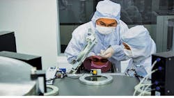
Dr. Gao Libo, the first author of the paper and a researcher with the Graphene Research Centre at NUS Faculty of Science, grew graphene on a copper catalyst layer coating a silicon substrate. After growth, the copper is etched away while the graphene is held in place by bubbles that form capillary bridges, similar to those seen around the feet of beetles and tree frogs attached to submerged leaves. The capillary bridges help to keep the graphene on the silicon surface and prevent its delamination during the etching of the copper catalyst. The graphene then attaches to the silicon layer.

To facilitate the formation of capillary bridges, a pre-treatment step involving the injection of gases into the wafer was applied by Dr. Gao. This helps to modify the properties of the interface and facilitates the formation of capillary bridges during the infiltration of a catalyst-removal liquid. The co-addition of surfactant helps to iron out any folds and creases that may be created during the transfer process.
Industrial And Other New Apps
This novel technique of growing graphene directly on silicon wafers and other stiff substrates will be very useful for the development of rapidly emerging graphene-on-silicon platforms, which have shown a promising range of applications. The "face-to-face transfer" method developed by the NUS team is also amenable to batch-processed semiconductor production lines, such as the fabrication of large-scale integrated circuits on silicon wafers.
To further their research, Prof Loh and his team will optimize the process in order to achieve high throughput production of large diameter graphene on silicon, as well as target specific graphene-enabled applications on silicon. The team is also applying the techniques to other two-dimensional films. Talks are now underway with potential industry partners.
About the Author

Sam Davis Blog
Editor-In-Chief - Power Electronics
Sam Davis was the editor-in-chief of Power Electronics Technology magazine and website that is now part of Electronic Design. He has 18 years experience in electronic engineering design and management, six years in public relations and 25 years as a trade press editor. He holds a BSEE from Case-Western Reserve University, and did graduate work at the same school and UCLA. Sam was the editor for PCIM, the predecessor to Power Electronics Technology, from 1984 to 2004. His engineering experience includes circuit and system design for Litton Systems, Bunker-Ramo, Rocketdyne, and Clevite Corporation.. Design tasks included analog circuits, display systems, power supplies, underwater ordnance systems, and test systems. He also served as a program manager for a Litton Systems Navy program.
Sam is the author of Computer Data Displays, a book published by Prentice-Hall in the U.S. and Japan in 1969. He is also a recipient of the Jesse Neal Award for trade press editorial excellence, and has one patent for naval ship construction that simplifies electronic system integration.
Comment About the Article
To join the conversation, and become an exclusive member of Electronic Design, create an account today!

Leaders relevant to this article: