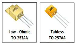
Please read the Important Notice and Warnings at the end of this document www.infineon.com/irhirel page 1 of 15 2022-12-13 IRHYS9A97230CM, IRHYB9A97230CM PD-97960B Radiation Hardened Power MOSFET Thru-Hole (Low-Ohmic TO-257AA) -200V, -14A, P-channel, R9 Superjunction Technology Features Single event effect (SEE) hardened (up to LET of 90.5 MeV·cm2/mg) Improved SOA for linear mode operation Low RDS(on) Improved avalanche energy Simple drive requirements Hermetically sealed Electrically isolated Ceramic eyelets ESD rating: class 2 per MIL-STD-750, Method 1020 Potential Applications Motor drives DC-DC converter Latching current limiter Product Validation Qualified according to MIL-PRF-19500 for space applications Description IR HiRel R9 technology provides superior power MOSFETs for space applications. This family of p-channel MOSFETs are the first radiation hardened devices that are based on a superjunction technology. These devices have improved immunity to Single Event Effect (SEE) and have been characterized for useful performance with Linear Energy Transfer (LET) up to 90.5 MeV·cm2/mg. Their combination of low RDS(on) and improved SOA allows for better performance in applications such as Latching Current Limiters (LCL), Solid-State Power Controllers (SSPC) or DC- DC converters. These devices retain all of the well-established advantages of MOSFETs such as voltage control, fast switching and temperature stability of electrical parameters. Ordering Information Table 1 Ordering options Part number Package Screening Level TID Level IRHYS9A97230CM Low-Ohmic TO-257AA COTS 100 krad(Si) JANSR2N7661T3 Low-Ohmic TO-257AA JANS 100 krad(Si) IRHYS9A93230CM Low-Ohmic TO-257AA COTS 300 krad(Si) JANSF2N7661T3 Low-Ohmic TO-257AA JANS 300 krad(Si) IRHYB9A97230CM Tabless TO-257AA COTS 100 krad(Si) JANSR2N7661D5 Tabless TO-257AA JANS 100 krad(Si) IRHYB9A93230CM Tabless TO-257AA COTS 300 krad(Si) JANSF2N7661D5 Tabless TO-257AA JANS 300 krad(Si) Low – Ohmic TO-257AA Product Summary BVDSS: -200V ID : -14A RDS(on),max : 175m QG,max : 49nC REF: MIL-PRF-19500/780 Tabless TO-257AA 2 of 15 2022-12-13 IRHYS9A97230CM, IRHYB9A97230CM Radiation Hardened Power MOSFET Thru-Hole (Low- Ohmic TO-257AA) Table of contents Table of contents Features ........................................................................................................................................ 1 Potential Applications ..................................................................................................................... 1 Product Validation .......................................................................................................................... 1 Description .................................................................................................................................... 1 Ordering Information ...................................................................................................................... 1 Table of contents ............................................................................................................................ 2 1 Absolute Maximum Ratings ..................................................................................................... 3 2 Device Characteristics ............................................................................................................ 4 2.1 Electrical Characteristics (Pre-Irradiation) ............................................................................................. 4 2.2 Source-Drain Diode Ratings and Characteristics (Pre-Irradiation) ....................................................... 5 2.3 Thermal Characteristics .......................................................................................................................... 5 2.4 Radiation Characteristics ........................................................................................................................ 5 2.4.1 Electrical Characteristics — Post Total Dose Irradiation .................................................................. 5 2.4.2 Single Event Effects — Safe Operating Area ...................................................................................... 6 3 Electrical Characteristics Curves (Pre-irradiation) ..................................................................... 7 4 Test Circuits (Pre-irradiation) ................................................................................................. 11 5 Package Outline (Low-Ohmic TO-257AA) .................................................................................. 12 6 Package Outline (Tabless TO-257AA) ....................................................................................... 13 Revision history............................................................................................................................. 14 3 of 15 2022-12-13 IRHYS9A97230CM, IRHYB9A97230CM Radiation Hardened Power MOSFET Thru-Hole (Low- Ohmic TO-257AA) Absolute Maximum Ratings 1 Absolute Maximum Ratings Table 2 Absolute Maximum Ratings (Pre-Irradiation) 1 Repetitive Rating; Pulse width limited by maximum junction temperature. 2 VDD = -125V, starting TJ = 25°C, L = 19mH, Peak IL = -9A, VGS = -20V 3 ISD -14A, di/dt -905A/μs, VDD -200V, TJ 150°C Symbol Parameter Value Unit ID1 @ VGS = -12V, TC = 25°C Continuous Drain Current -14 A ID2 @ VGS = -12V, TC = 100°C Continuous Drain Current -9.0 A IDM @ TC = 25°C Pulsed Drain Current 1 -56 A PD @ TC = 25°C Maximum Power Dissipation 75 W Linear Derating Factor 0.6 W/°C VGS Gate-to-Source Voltage ± 20 V EAS Single Pulse Avalanche Energy 2 770 mJ IAR Avalanche Current 1 -9.0 A EAR Repetitive Avalanche Energy 1 7.5 mJ dv/dt Peak Diode Reverse Recovery 3 -20 V/ns TJ TSTG Operating Junction and Storage Temperature Range -55 to +150 °C Lead Temperature 300 (0.063in./1.6mm from case for 10s) Weight 4.3 (Typical) g 4 of 15 2022-12-13 IRHYS9A97230CM, IRHYB9A97230CM Radiation Hardened Power MOSFET Thru-Hole (Low- Ohmic TO-257AA) Device Characteristics 2 Device Characteristics 2.1 Electrical Characteristics (Pre-Irradiation) Table 3 Static and Dynamic Electrical Characteristics @ Tj = 25°C (Unless Otherwise Specified) Symbol Parameter Min. Typ. Max. Unit Test Conditions BVDSS Drain-to-Source Breakdown Voltage -200 — — V VGS = 0V, ID = -1.0mA BVDSS/TJ Breakdown Voltage Temp. Coefficient — -0.22 — V/°C Reference to 25°C, ID = -1.0mA RDS(on) Static Drain-to-Source On-State Resistance — — 175 m VGS = -12V, ID2 = -9A 1 VGS(th) Gate Threshold Voltage -2.0 — -4.0 V VDS ≥ VGS, ID = -1mA VGS(th)/TJ Gate Threshold Voltage Coefficient — 5.0 — mV/°C Gfs Forward Transconductance 5.4 — — S VDS = -15V, ID2 = -9A 1 IDSS Zero Gate Voltage Drain Current — — -10 A VDS = -160V, VGS = 0V — — -25 VDS = -160V, VGS = 0V, TJ = 125°C IGSS Gate-to-Source Leakage Forward — — -100 nA VGS = -20V Gate-to-Source Leakage Reverse — — 100 VGS = 20V QG Total Gate Charge — — 49 nC ID1 = -14A VDS = -100V VGS = -12V QGS Gate-to-Source Charge — — 16 QGD Gate-to-Drain (‘Miller’) Charge — — 12 td(on) Turn-On Delay Time — — 18 ns ID1 = -14A ** VDD = -100V RG = 7.5 VGS = -12V tr Rise Time — — 30 td(off) Turn-Off Delay Time — — 84 tf Fall Time — — 30 Ls +LD Total Inductance — 6.8 — nH Measured from Drain lead (6mm / 0.25in. from package) to Source lead (6mm / 0.25in. from package) with Source wires internally bonded from Source Pin to Drain Pad Ciss Input Capacitance — 2215 — pF VGS = 0V VDS = -25V ƒ = 1.0MHz Coss Output Capacitance — 270 — Crss Reverse Transfer Capacitance — 6.0 — RG Gate Resistance — 5.0 — ƒ = 1.0MHz, open drain ** Switching speed maximum limits are based on manufacturing test equipment and capability. 1 Pulse width 300 μs; Duty Cycle 2% 5 of 15 2022-12-13 IRHYS9A97230CM, IRHYB9A97230CM Radiation Hardened Power MOSFET Thru-Hole (Low- Ohmic TO-257AA) Device Characteristics 2.2 Source-Drain Diode Ratings and Characteristics (Pre-Irradiation) Table 4 Source-Drain Diode Characteristics Symbol Parameter Min. Typ. Max. Unit Test Conditions IS Continuous Source Current (Body Diode) — — -14 A ISM Pulsed Source Current (Body Diode) 1 — — -56 A VSD Diode Forward Voltage — — -1.3 V TJ = 25°C, IS = -14A, VGS = 0V 2 trr Reverse Recovery Time — 159 239 ns TJ = 25°C, IF = -14A, VDD ≤ -25V di/dt = -100A/μsQrr Reverse Recovery Charge — 1.1 — C ton Forward Turn-On Time Intrinsic turn-on time is negligible (turn-on is dominated by LS+LD) 2.3 Thermal Characteristics Table 5 Thermal Resistance Symbol Parameter Min. Typ. Max. Unit RJC Junction-to-Case — — 1.67 °C/W RJA Junction-to-Ambient — — 80 2.4 Radiation Characteristics IR HiRel Radiation Hardened MOSFETs are tested to verify their radiation hardness capability. The hardness assurance program at IR HiRel is comprised of two radiation environments. Every manufacturing lot is tested for total ionizing dose (per notes 3 and 4) using the TO-3 package. Both pre- and post-irradiation performance are tested and specified using the same drive circuitry and test conditions in order to provide a direct comparison. 2.4.1 Electrical Characteristics — Post Total Dose Irradiation Table 6 Electrical Characteristics @ Tj = 25°C, Post Total Dose Irradiation 3, 4 Symbol Parameter Up to 300krads (Si)5 Unit Test Conditions Min. Max. BVDSS Drain-to-Source Breakdown Voltage -200 — V VGS = 0V, ID = -1mA VGS(th) Gate Threshold Voltage -2.0 -4.0 V VDS ≥ VGS, ID = -1mA IGSS Gate-to-Source Leakage Forward — -100 nA VGS = -20V Gate-to-Source Leakage Reverse — 100 VGS = 20V IDSS Zero Gate Voltage Drain Current — -10 μA VDS = -160V, VGS = 0V RDS(on) Static Drain-to-Source On-State Resistance (TO-3) 2 — 175 m VGS = -12V, ID2 = -9A RDS(on) Static Drain-to-Source On-State Resistance (Low-Ohmic TO-257AA)2 — 175 m VGS = -12V, ID2 = -9A VSD Diode Forward Voltage — -1.3 V VGS = 0V, IF = -14A 1 Repetitive Rating; Pulse width limited by maximum junction temperature. 2 Pulse width 300 μs; Duty Cycle 2% 3 Total Dose Irradiation with VGS Bias. VGS =- 12V applied and VDS = 0 during irradiation per MIL-STD-750, Method 1019, condition A. 4 Total Dose Irradiation with VDS Bias. VDS = -160V applied and VGS = 0 during irradiation per MlL-STD-750, Method 1019, condition A. 5 Part numbers IRHYS9A97230CM (JANSR2N7661T3), IRHYS9A93230CM (JANSF2N7661T3), IRHYB9A97230CM (JANSR2N7661D5), and IRHYB9A93230CM (JANSF2N7661D5) 6 of 15 2022-12-13 IRHYS9A97230CM, IRHYB9A97230CM Radiation Hardened Power MOSFET Thru-Hole (Low- Ohmic TO-257AA) Device Characteristics 2.4.2 Single Event Effects — Safe Operating Area IR HiRel radiation hardened MOSFETs have been characterized in heavy ion environment for Single Event Effects (SEE). Single Event Effects characterization is illustrated in Fig. 1 and Table 7. Table 7 Typical Single Event Effects Safe Operating Area LET (MeV·cm2/mg) Energy (MeV) Range (μm) VDS (V) VGS = 0V VGS = 3V VGS = 5V VGS = 10V 38.4 ± 5% 420± 7.5% 51.9 ± 7.5% -200 -200 -200 -200 66.4 ± 5% 783 ± 7.5% 59.4 ± 7.5% -200 -200 -200 — 90.5 ± 5% 1430 ± 7.5% 80.4± 7.5% -200 -200 — — Figure 1 Typical Single Event Effect, Safe Operating Area 7 of 15 2022-12-13 IRHYS9A97230CM, IRHYB9A97230CM Radiation Hardened Power MOSFET Thru-Hole (Low- Ohmic TO-257AA) Electrical Characteristics Curves (Pre-irradiation) 3 Electrical Characteristics Curves (Pre-irradiation) Figure 2 Typical Output Characteristics Figure 3 Typical Output Characteristics Figure 4 Typical Transfer Characteristics Figure 5 Normalized On-Resistance Vs. Temperature 8 of 15 2022-12-13 IRHYS9A97230CM, IRHYB9A97230CM Radiation Hardened Power MOSFET Thru-Hole (Low- Ohmic TO-257AA) Electrical Characteristics Curves (Pre-irradiation) Figure 6 Typical On-Resistance Vs. Gate Voltage Figure 7 Typical On-Resistance Vs. Drain Current Figure 8 Typical Drain-to-Source Breakdown Voltage Vs. Temperature Figure 9 Typical Threshold Voltage Vs. Temperature 9 of 15 2022-12-13 IRHYS9A97230CM, IRHYB9A97230CM Radiation Hardened Power MOSFET Thru-Hole (Low- Ohmic TO-257AA) Electrical Characteristics Curves (Pre-irradiation) Figure 10 Typical Capacitance Vs. Drain-to-Source Voltage Figure 11 Typical Gate-to-Source Voltage Vs. Gate Charge Figure 12 Typical Source-Drain Current Vs. Diode Forward Voltage Figure 13 Maximum Drain Current Vs. Case Temperature 10 of 15 2022-12-13 IRHYS9A97230CM, IRHYB9A97230CM Radiation Hardened Power MOSFET Thru-Hole (Low- Ohmic TO-257AA) Electrical Characteristics Curves (Pre-irradiation) Figure 14 Maximum Safe Operating Area Figure 15 Maximum Safe Operating Area Figure 16 Maximum Avalanche Energy Vs. Junction Temperature Figure 17 Maximum Effective Transient Thermal Impedance, Junction-to-Case 11 of 15 2022-12-13 IRHYS9A97230CM, IRHYB9A97230CM Radiation Hardened Power MOSFET Thru-Hole (Low- Ohmic TO-257AA) Test Circuits (Pre-irradiation) 4 Test Circuits (Pre-irradiation) Figure 18 Gate Charge Test Circuit Figure 19 Gate Charge Waveform Figure 20 Unclamped Inductive Test Circuit Figure 21 Unclamped Inductive Waveform Figure 22 Switching Time Test Circuit Figure 23 Switching Time Waveforms 12 of 15 2022-12-13 IRHYS9A97230CM, IRHYB9A97230CM Radiation Hardened Power MOSFET Thru-Hole (Low- Ohmic TO-257AA) Package Outline (Low-Ohmic TO-257AA) 5 Package Outline (Low-Ohmic TO-257AA) Note: For the most updated package outline, please see the website: (Low-Ohmic TO-257AA) BERYLLIA WARNING PER MIL-PRF-19500 Package containing beryllia shall not be ground, sandblasted, machined, or have other operations performed on them which will produce beryllia or beryllium dust. Furthermore, beryllium oxide packages shall not be placed in acids that will produce fumes containing beryllium. 13 of 15 2022-12-13 IRHYS9A97230CM, IRHYB9A97230CM Radiation Hardened Power MOSFET Thru-Hole (Low- Ohmic TO-257AA) Package Outline (Tabless TO-257AA) 6 Package Outline (Tabless TO-257AA) Note: For the most updated package outline, please see the website: Tabless TO-257AA BERYLLIA WARNING PER MIL-PRF-19500 Package containing beryllia shall not be ground, sandblasted, machined, or have other operations performed on them which will produce beryllia or beryllium dust. Furthermore, beryllium oxide packages shall not be placed in acids that will produce fumes containing beryllium. 14 of 15 2022-12-13 IRHYS9A97230CM, IRHYB9A97230CM Radiation Hardened Power MOSFET Thru-Hole (Low- Ohmic TO-257AA) Revision history Revision history Document version Date of release Description of changes 10/19/2022 Preliminary datasheet with PPD number (PPD-97960A) Rev B 12/13/2022 Final datasheet with PD number Edition 2022-12-13 Published by International Rectifier HiRel Products, Inc. An Infineon Technologies company El Segundo, California 90245 USA © 2022 Infineon Technologies AG. All Rights Reserved. Do you have a question about this document? Email: [email protected] Document reference IMPORTANT NOTICE The information given in this document shall in no event be regarded as a guarantee of conditions or characteristics (“Beschaffenheitsgarantie”). With respect to any examples, hints or any typical values stated herein and/or any information regarding the application of the product, Infineon Technologies hereby disclaims any and all warranties and liabilities of any kind, including without limitation warranties of non-infringement of intellectual property rights of any third party. In addition, any information given in this document is subject to customer’s compliance with its obligations stated in this document and any applicable legal requirements, norms and standards concerning customer’s products and any use of the product of Infineon Technologies in customer’s applications. The data contained in this document is exclusively intended for technically trained staff. It is the responsibility of customer’s technical departments to evaluate the suitability of the product for the intended application and the completeness of the product information given in this document with respect to such application. For further information on the product, technology, delivery terms and conditions and prices please contact your nearest Infineon Technologies office (www.infineon.com). WARNINGS Due to technical requirements components may contain dangerous substances. For information on the types in question please contact your nearest International Rectifier HiRel Products, Inc., an Infineon Technologies company, office. International Rectifier HiRel Components may only be used in life-support devices or systems with the expressed written approval of International Rectifier HiRel Products, Inc., an Infineon Technologies company, if failure of such components can reasonably be expected to cause the failure of that life-support device or system, or to affect the safety and effectiveness of that device or system. Life support devices or systems are intended to be implanted in the human body, or to support and/or maintain and sustain and/or protect human life. If they fail, it is reasonable to assume that the health of the user or other persons may be endangered. Trademarks All referenced product or service names and trademarks are the property of their respective owners.