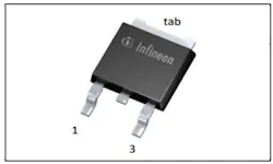
Datasheet Please read the Important Notice and Warnings at the end of this document IFAG PSS RFS D HIR www.infineon.com 1 of 10 Issue 4.1, April 2026 BUP06CP038F-01 60V p-channel radiation tolerant power MOSFET BUP06CP038F-01 Features • Low RDS(on) • Single Event Effect (SEE) tolerant up to Linear Energy Transfer (LET) = 46 MeVcm2/mg • Total Ionisation Dose (TID) tolerant up to 30 kRad(Si) • P-channel Product validation Qualified for space applications according to the relevant tests of AEC-Q101 TID irradiation according to ESCC 22900 standard1 Description Table 1 Product information Type Comment Pin Configuration Package 1 2 (tab) 3 BUP06CP038F-01 G D S DPAK (TO252) 1 TID irradiation testing for this device conforms to the ESCC 22900 standard. Parameters specified in this datasheet reflect post irradiation performance only. Rad report can be provided by request. Please contact sales to request a report. Datasheet 2 of 10 Issue 4.1, April 2026 60V p-channel radiation tolerant power MOSFET BUP06CP038F-01 Table of contents Table of contents Features ....................................................................................................................................... 1 Product validation .......................................................................................................................... 1 Description .................................................................................................................................... 1 Table of contents ............................................................................................................................ 2 1 Maximum ratings ................................................................................................................... 3 2 Thermal characteristics .......................................................................................................... 4 3 Electrical characteristics ......................................................................................................... 5 4 Electrical characteristics diagrams........................................................................................... 6 5 Package outlines and footprint ................................................................................................ 9 Datasheet 3 of 10 Issue 4.1, April 2026 60V p-channel radiation tolerant power MOSFET BUP06CP038F-01 Maximum ratings 1 Maximum ratings Table 2 Maximum ratings Parameter Symbol Values Unit Note / Test Condition Min. Typ. Max. Drain source voltage VDS - - -60 V Gate source voltage VGS -20 - 20 V static Drain gate voltage VDG - - -60 V Continuous drain current 1 ID - - - - -35 -28 A TC = 25 °C TC = 100 °C Continuous source current IS - - -35 A Drain current pulsed IDM - - -140 Apk Total power dissipation 2 Ptot - - 125 W TC ≤ 25 °C Operating temperature Top -55 - 175 °C Junction temperature Tj -55 - 175 °C Storage temperature Tstg -55 - 175 °C Avalanche energy EAS - - 500 mJ ID = -35 A, RGS = 25 Ω 1 Limited by junction temperature 2 For TC > 25°C derating is required. Datasheet 4 of 10 Issue 4.1, April 2026 60V p-channel radiation tolerant power MOSFET BUP06CP038F-01 Thermal characteristics 2 Thermal characteristics Table 3 Thermal characteristics Parameter Symbol Values Unit Note / Test Condition Min. Typ. Max. Thermal resistance, junction - case Rth,JC - - 1.2 K/W Thermal resistance, junction - ambient Rth,JA - - 75 K/W Device on 40 mm x 40 mm x 1.5 mm epoxy PCB FR4 with 6 cm2 (one layer, 70 μm thickness) copper area for drain connection. PCB is vertical without air stream cooling Soldering temperature Tsol - - 260 °C 1.6 mm (0.063 in.) from case for 10 s Datasheet 5 of 10 Issue 4.1, April 2026 60V p-channel radiation tolerant power MOSFET BUP06CP038F-01 Electrical characteristics 3 Electrical characteristics at TA =25 °C, unless otherwise specified Table 4 Static characteristics Parameter Symbol Values Unit Note / Test Condition Min. Typ. Max. Drain-source breakdown voltage BVDSS -60 - - V ID = 1 mA, VGS = 0 V Gate threshold voltage VGS(th) -2 -3 -5 V ID = -1.7 mA, VDS = VGS Gate to source leakage current IGSS - -10 -100 nA VDS = 0 V, VGS = +/- 20 V Zero gate voltage drain current IDSS - - -0.1 -10 -1 -100 μA VDS = -48 V, VGS = 0 V, TA = 25 °C VDS = -48 V, VGS = 0 V, TA = 125 °C Drain source on-state resistance 1 RDS(ON) - 32 38 mΩ VGS = -10 V, ID = -35 A Diode forward voltage VSD - -1.2 -1.6 V VGS = 0 V, IS = -35 A Table 5 Dynamic characteristics Parameter Symbol Values Unit Note / Test Condition Min. Typ. Max. Turn-on delay time td(ON) - 16 - ns VDD = -30 V, VGS = -10 V, ID = -17.5 A, RG = 1.6 Ω Rise time tr - 19 - ns VDD = -30 V, VGS = -10 V, ID = -17.5 A, RG = 1.6 Ω Turn-off delay time td(OFF) - 47 - ns VDD = -30 V, VGS = -10 V, ID = -17.5 A, RG = 1.6 Ω Fall time tf - 19 - ns VDD = -30 V, VGS = -10 V, ID = -17.5 A, RG = 1.6 Ω Reverse recovery time trr - 63 - ns VDD = -30V, IF = IS, diF/dt = 100 A/μs Common source input capacitance Ciss - 2.5 - nF VDS = -30 V, VGS = 0 V, f = 1.0 MHz Common source output capacitance Coss - 0.36 - nF VDS = -30 V, VGS = 0 V, f = 1.0 MHz Common source reverse transfer capacitance Crss - 83 - pF VDS = -30 V, VGS = 0 V, f = 1.0 MHz Total gate charge QG - 63 - nC VDD = -30 V, VGS = 0 to -10 V, ID = -35 A 1 Pulsed measurement: Pulse Width < 300 μs, Duty Cycle < 2.0%. Datasheet 6 of 10 Issue 4.1, April 2026 60V p-channel radiation tolerant power MOSFET BUP06CP038F-01 Electrical characteristics diagrams 4 Electrical characteristics diagrams Diagram 1: Safe operating area Diagram 2: Max. transient thermal impedance ID = f(VDS); TC = 25 °C; D=0; parameter: tp ZthJC = f(tp); parameter: D = tp/T Diagram 3: Typ. output characteristics Diagram 4: Typ. drain-source on-state resistance ID = f(VDS); Tj = 25 °C; parameter: VGS RDS(on) = f(Tj); ID =-35 A; VGS = -10 V Datasheet 7 of 10 Issue 4.1, April 2026 60V p-channel radiation tolerant power MOSFET BUP06CP038F-01 Electrical characteristics diagrams Diagram 5: Typ. drain-source on-state resistance Diagram 6: Typ. transfer characteristics RDS(on) = f(ID); Tj = 25 °C; parameter: VGS ID = f(VGS), VDS ≥ 2 x ID x RDS(on)max; parameter: Tj Diagram 7: Typ. gate threshold voltage Diagram 8: Forward characteristics of reverse diode ID = f(Tj); VGS = VDS ; parameter: ID IF = f(VSD); parameter: Tj Datasheet 8 of 10 Issue 4.1, April 2026 60V p-channel radiation tolerant power MOSFET BUP06CP038F-01 Electrical characteristics diagrams Diagram 9: Drain-source breakdown voltage Diagram 10: Typ. capacitances BVDSS = f(Tj); ID = -250 μA C = f(VDS); VGS = 0 V; f = 1 MHz Diagram 11: Typ. gate charge Diagram 12: SEE – Safe operating area VGS = f(Qgate); ID = -35.0 A pulsed; parameter: VDD Datasheet 9 of 10 Issue 4.1, April 2026 60V p-channel radiation tolerant power MOSFET BUP06CP038F-01 Package outlines and footprint 5 Package outlines and footprint Trademarks All referenced product or service names and trademarks are the property of their respective owners. Edition 4.1, April 2026 Published by Infineon Technologies AG 81726 München, Germany © 2026 Infineon Technologies AG. All Rights Reserved. Do you have a question about this document? Email: [email protected] IMPORTANT NOTICE The information given in this document shall in no event be regarded as a guarantee of conditions or characteristics (“Beschaffenheitsgarantie”) . With respect to any examples, hints or any typical values stated herein and/or any information regarding the application of the product, Infineon Technologies hereby disclaims any and all warranties and liabilities of any kind, including without limitation warranties of non-infringement of intellectual property rights of any third party. In addition, any information given in this document is subject to customer’s compliance with its obligations stated in this document and any applicable legal requirements, norms and standards concerning customer’s products and any use of the product of Infineon Technologies in customer’s applications. The data contained in this document is exclusively intended for technically trained staff. It is the responsibility of customer’s technical departments to evaluate the suitability of the product for the intended application and the completeness of the product information given in this document with respect to such application. For further information on the product, technology, delivery terms and conditions and prices please contact your nearest Infineon Technologies office (www.infineon.com). WARNINGS Due to technical requirements products may contain dangerous substances. For information on the types in question please contact your nearest Infineon Technologies office. Infineon Technologies Components may only be used in life-support devices or systems with the expressed written approval of Infineon Technologies, if a failure of such components can reasonably be expected to cause the failure of that life-support device or system, or to affect the safety or effectiveness of that device or system. Life support devices or systems are intended to be implanted in the human body, or to support and/or maintain and sustain and/or protect human life. If they fail, it is reasonable to assume that the health of the user or other persons may be endangered. Datasheet 10 of 10 Issue 4.1, April 2026 60V p-channel radiation tolerant power MOSFET BUP06CP038F-01