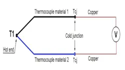
Application Note Thermocouple Cold Junction Compensation SLG47011 R19AN0341EE0100 Rev.1.00 Sep 23, 2024 Page 1 © 2024 Renesas Electronics This application note describes how to design and build a thermocouple signal conditioner with PGA, 12-bit ADC with I²C interface, and cold junction compensation using an onboard temp sensor. The device is built on the SLG47011. The IC is equipped with the PGA (gain up to 64x), 14-bit ADC (12-bit mode is used in this case), analog Temp Sensor, Data Buffers (used to average measurements), Memory Table (used to align temp sensor data with the thermocouple), and Math Core which does the required calculations. In addition, the SLG47011 contains a huge amount of different macrocells, allowing almost any additional function to be added. The application note comes complete with a design file that can be found in the Reference section. Contents 1. Terms and Definitions ................................................................................................................................... 2 2. References...................................................................................................................................................... 2 3. Introduction .................................................................................................................................................... 3 3.1 Thermocouple Theory ........................................................................................................................... 3 3.2 Thermocouple Types and Materials ...................................................................................................... 3 3.3 Thermovoltage ....................................................................................................................................... 5 3.4 Seebeck Coefficients ............................................................................................................................. 6 3.5 Cold Junction Compensation ................................................................................................................. 6 4. Automatic Cold Junction Compensation .................................................................................................... 7 4.1 Theory of Operation ............................................................................................................................... 7 4.1.1. DAC ......................................................................................................................................... 7 4.1.2. Programmable Gain Amplifier ................................................................................................. 7 4.1.3. Analog Temperature Sensor ................................................................................................... 8 4.1.4. Analog-to-Digital Converter ..................................................................................................... 8 4.1.5. Counter Delay (CNT/DLY) ...................................................................................................... 9 4.1.6. Data Buffers ............................................................................................................................ 9 4.1.7. Memory Table ......................................................................................................................... 9 4.1.8. Mathematical Core ................................................................................................................ 10 4.2 AnalogPAK Project .............................................................................................................................. 11 4.2.1. PIN Configuration .................................................................................................................. 11 4.2.2. DAC Settings ......................................................................................................................... 11 4.2.3. Temp Sensor Settings ........................................................................................................... 11 4.2.4. PGA Configuration ................................................................................................................ 12 4.2.5. ADC Configuration ................................................................................................................ 12 4.2.6. Data Buffers Configuration .................................................................................................... 12 4.2.7. Memory Table Configuration ................................................................................................. 12 4.2.8. Math Core Configuration ....................................................................................................... 14 4.2.9. Counter/Delay Configuration ................................................................................................. 14 4.2.10. Oscillators Configuration ....................................................................................................... 14 4.2.11. LUT Settings ......................................................................................................................... 14 Thermocouple Cold Junction Compensation R19AN0341EE0100 Rev.1.00 Sep 23, 2024 Page 2 4.3 Reading the Data ................................................................................................................................. 14 5. Testing the Device ....................................................................................................................................... 15 6. Design Simulation ....................................................................................................................................... 15 7. Conclusions ................................................................................................................................................. 16 8. Revision History .......................................................................................................................................... 18 1. Terms and Definitions ADC Analog-to-Digital Converter CNT/DLY Counter-Delay DAC Digital-to-Analog Converter DCMP Digital Comparator FSM Finite State Machine IC Integrated Circuit I2C Inter-Integrated Circuit Protocol LSB Least Significant Bit MSB Most Significant Bit MUX Multiplexer NTC Negative Thermal Coefficient NVM Non-volatile Memory OSC Oscillator PCB Printed Circuit Board PGA Programable Gain Amplifier PTC Positive Thermal Coefficient PWM Pulse Width Modulation RAM Random-access Memory ROM Read-only Memory SAR Successive-approximation-register SCL Signal Clock SDA Signal Data TS Temperature Sensor 2. References For related documents and software, please visit: AnalogPAK™ | Renesas Download our free Go Configure Software Hub [1] to open the .aap file [2] and view the proposed circuit design. Use the GreenPAK development tools [3] to freeze the design into your own customized IC in a matter of minutes. Renesas Electronics provides a complete library of application notes [4] featuring design examples, as well as explanations of features and blocks within the Renesas IC. Thermocouple Cold Junction Compensation R19AN0341EE0100 Rev.1.00 Sep 23, 2024 Page 3 [1] GreenPAK Go Configure Software Hub, Software Download and User Guide, Renesas Electronics [2] AN-CM-389 Thermocouple Cold Junction Compensation, GreenPAK Design File, Renesas Electronics [3] GreenPAK Development Tools, GreenPAK Development Tools Webpage, Renesas Electronics [4] GreenPAK Application Notes, GreenPAK Application Notes Webpage, Renesas Electronics [5] SLG47011 Datasheet, Renesas Electronics [6] Thermocouple Cold (Reference) Junction Compensation [7] Type K Thermocouple [8] Thermocouple Voltage to Temperature Calculator 3. Introduction 3.1 Thermocouple Theory Thermocouple is a very common industry temperature sensor. It has a few benefits that make it widely used. Such as measuring very high temperatures, much higher than NTC or PTC resistors, robustness, so it does not break easily, and low price. Although thermocouples are not as accurate as mentioned N(P)TC sensors, they are accurate enough in many applications. There are many different thermocouple types optimized for different applications. A thermocouple consists of two wires made of different electrical conductors that are welded together at one end, the “hot” end. It generates a thermo-electric current, causing a small voltage between the wires in the open end. The voltage depends on the temperature and the materials of the conductive wires being used. This effect was named the Seebeck effect after its discoverer Thomas Johann Seebeck back in 1821. Figure 1: Thermocouple In Figure 1 the “Thermocouple materials 1 and 2” represent the two different materials the thermocouple is made of. “T1” is the hot end of the thermocouple, i.e. the point that is used to measure temperature. The two “Tcj” are the temperatures of the cold junctions. The thermovoltage is generated by the temperature gradients in the thermocouple wire, in both “hot” and “cold” junctions. 3.2 Thermocouple Types and Materials There are many types of thermocouples being manufactured from different materials and alloys. Different materials will cause different sensitivity, different amounts of generated thermovoltage at the same temperature, and will affect other characteristics such as max temperature. Several various thermocouple types have been standardized and names are given for specified used materials. For example: type K, R, S, J, K, etc., see Table 1 Thermocouple Cold Junction Compensation R19AN0341EE0100 Rev.1.00 Sep 23, 2024 Page 5 Table 1. Thermocouple Types and Materials Type Positive Wire Negative Wire B 70% Platinum 30% Rhodium 94% Platinum 6% Rhodium E Chromel Constantan J Iron Constantan K Chromel Alumel N Nicrosil Nisil R 87% Platinum 13% Rhodium Platinum S 90% Platinum 10% Rhodium Platinum T Copper Constantan 3.3 Thermovoltage As different thermocouples are made of different materials, the thermovoltage is also different, this is illustrated in Figure 2. There is a big difference in the voltage being generated at the same temperature between the different types. Figure 2: Emf vs Temperature The different sensitivities between different thermocouples also explain why thermocouple thermometers typically have different accuracy specifications for different thermocouple types. These devices normally have the voltage measurement accuracy specified in voltage. For example, it can have an accuracy of 4 μV. Due to the different Thermocouple Cold Junction Compensation R19AN0341EE0100 Rev.1.00 Sep 23, 2024 Page 6 thermocouple sensitivities, this 4-microvolt accuracy equals a different temperature accuracy depending on the thermocouple type. For example, the E and B type at 200 °C temperature. The sensitivity (Seebeck coefficient) of type E at 200 °C is about 74 μV/ °C, while the coefficient for B type at 200 °C is about 2 μV/ °C. So, there is a difference of 37 times between these two. So, if the measurement device (microvoltmeter) can measure with an electrical accuracy of 4 μV, it means that it offers an accuracy of about 0.05°C (4 μV divided by 74 μV/°C) for the E type at 200°C and accuracy of 2°C (4 μV divided by 2 μV/°C) with B type at 200°C. 3.4 Seebeck Coefficients The Seebeck coefficient is the sensitivity of the thermocouple, i.e. it explains how much voltage is generated per temperature change, see Figure 3. Figure 3: Seebeck Coefficients 3.5 Cold Junction Compensation As shown in Figure 1, the thermocouple has a “hot” (measuring) end and two “cold” connections. During the measuring process, both “hot” and “cold” contacts generate voltage. So, to accurately measure the temperature at the “hot” end, the cold junction voltage must be considered. The cold junction voltage is generated in two points of contact: metal 1 with copper and metal 2 with copper. Instead of copper any metal or alloy can be used, the thermocouple’s cold ends can be connected to the voltmeter via gold-plated contacts or soldered directly to the PCB. It doesn’t matter, as long as both contacts are made of the same metal, they can be eliminated thus cold junction voltage is the same as between metal 1 and metal 2. By its nature, a thermocouple junction does not generate any thermovoltage when it is at 0°C temperature, see Figure 2. So, if the cold junction is placed in an electrically isolated ice bath or an accurate temperature block of 0°C, no compensation is needed. But this is not practical. The best way to compensate for the thermocouple cold junction is by measuring the temperature of the cold contacts (using a separate temp sensor), and converting that temperature into the thermocouple voltage, then using this value and the voltmeter readings to calculate the temperature at the hot end. See the example below. Thermocouple Cold Junction Compensation R19AN0341EE0100 Rev.1.00 Sep 23, 2024 Page 7 Example: Type K thermocouple is used. Voltmeter readings are: 21497 μV. The temperature of the cold junction is 20 °C. Using formula: E = EN(tU1) – EN(tr), Where: E - measured voltage = 19792 μV EN(tU1) - voltage generated by the hot end EN(tr) - voltage generated in cold junction = 798 μV (ITC-90 Table for K type Thermocouple, 20 °C) EN(tU1) = E + EN(tr) = 19792 μV + 798 μV = 20590 μV ≈ 498 °C (ITC-90 Table for K type Thermocouple, 20590 μV) We get the measured temperature of 498 °C. 4. Automatic Cold Junction Compensation 4.1 Theory of Operation Using the SLG47011 IC it is possible to build a thermocouple ADC with integrated cold junction compensation. Thanks to its collection of internal macro cells, the device has all the required parts which eliminates any external components, see the block diagram in Figure 4. Figure 4: Automatic Cold Junction Compensation Block Diagram 4.1.1. DAC Although the DAC is a fully functional macrocell, in this case, it is used in static mode to provide a voltage shift for the PGA in differential mode. A static value of 2048 results in an output voltage of ½ the internal Vref (810 mV). 4.1.2. Programmable Gain Amplifier The programmable Gain Amplifier (PGA) macrocell amplifies small signals. PGA has a 7-bit gain selection. Possible gain settings are 2x, 4x, 8x, 16x, 32x, 64x. It is also possible to bypass the PGA and measure signals Thermocouple Cold Junction Compensation R19AN0341EE0100 Rev.1.00 Sep 23, 2024 Page 8 directly with ADC. The PGA is rail-to-rail input and output and has a variety of different modes and settings. But in this project, only three of four channels are used. Two channels 0 and 1 (PINs 8, 12, and 7, 11 respectively) are set to a Differential input Instrumentation amplifier mode with 32x gain. Channel 0 is used for calibration which reduces PGA offset and noise error. Channel 1 is used for the measurement. The Differential input Instrumentation amplifier mode has the advantage of compensating the input noise, which increases the measurement accuracy. Channel 2 is used to input the TS voltage. It is set to Single-ended input, Buffer mode, and 1x gain. 4.1.3. Analog Temperature Sensor The SLG47011 IC is equipped with an internal analog temp sensor (TS), which is essential for the design as it plays the central part of the compensation. It should be mentioned that as the temp sensor is inside the IC, it must be placed in close proximity to the cold junction ensuring that the temperature of both is equal. The TS has output voltage linearly proportional to the Centigrade temperature. It is rated to operate over a -40 °C to 85 °C temperature range, which is perfect for the project. The output voltage can be calculated using the following formula: EN(tr) = 0.7538 - 0.00183×tr Where: EN(tr) - voltage generated in cold junction, V tr - TS (cold junction) temperature, °C 4.1.4. Analog-to-Digital Converter The SLG47011 has a successive approximation Analog-to-Digital Converter (SAR ADC) macrocell with configurable resolution of 14-bit, 12-bit, 10-bit, and 8-bit (12-bit mode is used in this project). It has an internal Sampling Engine block that switches input analog MUX and controls the ADC data receivers (Data Buffers or Memory Table macrocell). The input signal can be amplified through the PGA which has register gain, speed, and noise/power options configurable for each logical channel. ADC can sample up to four logical channels. Each logical channel is configured to operate with any possible analog input. ADC data destination options are: • Data Buffers (Data Buffer 3 option used in this project) • Address input of Memory Table macrocell (ROM mode used in this project) • Data input of Memory Table macrocell (RAM mode) • MathCore inputs (used in this project) • Internal one-word buffer accessible via I2C/SPI Host interface ADC voltage reference sources are: • External source (GPIO11) • Internal reference 1.62 V (used in this project) • Internal Vref divider (60 taps) • AVDD divider. ADC clock sources are: • Internal OSC 20/40 MHz • External clock from matrix • Configurable clock divider (/32 divider is used in this project) Thermocouple Cold Junction Compensation R19AN0341EE0100 Rev.1.00 Sep 23, 2024 Page 9 4.1.5. Counter Delay (CNT/DLY) This design uses three CNT/DLYs each part of a separate Multifunction Macrocell. CNT4/DLY4 makes a 200 ms ADC power-on delay to ensure its proper start-up initialization. CNT3/DLY3 and CNT2/DLY2 create a series of pulses that forces the ADC to calibrate itself every second. This technique ensures accurate measurements in a variable environment. 4.1.6. Data Buffers The SLG47011 has four Data Buffers (three used in this project) designed to store or process data from the ADC, Math Core, or CNT/DLY. In this project, the input sources for Data Buffers are: • Data Buffer 1 – Math Core • Data Buffer 2 – Data Buffer 1 (daisy chain with Data Buffer 1) • Data Buffer 3 – ADC Data (for TS readings) The user can select Data Buffer length 1, 2, 4, or 8 words, as well as the initial data of Data Buffers (0000h or FFFFh). The basic modes for Data Buffer are: • Storage mode • Moving Average mode (used in this project) • Oversampling mode In Moving Average mode, the number of samples, N, are taken from the Data Buffer DATA, added together, and the result is divided by N and written to the Buffer Result. The result is updated after each new data is loaded to the Data Buffer. This feature allows for eliminating noise in the measured signal. 4.1.7. Memory Table The Memory Table macrocell is a memory block that consists of 4096 12-bit words. It has 12-bit address and 12- bit data port. The address of each particular word comes from the address input, and its content is available after some propagation delay and access time at the output. The maximum clock speed for the Memory Table is 20 MHz. Memory Table can work in two modes: read-only memory (ROM; data in which is taken from NVM at chip startup) and randomized access memory (RAM; works as a storage block). Data in all modes can be rewritten via the I²C or SPI interfaces. The address input source for the Memory Table can be selected from: • Data Buffer0 • Data Buffer1 • Internal counter (must be selected when operating in RAM mode only) • ADC channels 0 to 3 (channel 2 used in this project) • Memory control counter • I²C /SPI host interface. The data input source can be selected from: • Data Buffer0 • ADC channels 0 to 3 • NVM (used in this project) • I2C/SPI host interface. Thermocouple Cold Junction Compensation R19AN0341EE0100 Rev.1.00 Sep 23, 2024 Page 10 Data output can be sourced to: • DAC • PWM • CNT/DLY 9 • MathCore (used in this project) • DCMP • Width Converter In this design, the Memory Table is set to ROM mode in which data from ADC channel 2 is converted to the Memory Table address. Output data of the Memory Table will be the contents of the pre-written addressed cell. 4.1.8. Mathematical Core The SLG47011 has a Mathematical core (MathCore) macrocell which allows it to perform four mathematical operations: addition, subtraction, multiplication, and division (cyclic shift), as well as their combinations. The function to be calculated by the MathCore can be selected by the user according to one of the following operation modes: • Multiplier and shifter mode • Adder/Subtractor mode • Multiplier + Adder/Subtractor mode (used in this project) • Adder/Subtractor + Multiplier mode Input sources for the MathCore can be: • ADC channel 0 output • ADC channel 1 output (used in this project) • ADC channel 2 output • ADC channel 3 output • Memory Table macrocell output (used in this project) • Data Buffer0 output • Data Buffer1 output • Data Buffer2 output • Constant K from Register (used in this project) • Constant B from Register In this design, MathCore is used to add data from the ADC channel 1 to data from the Memory Table. The result of this mathematical operation goes through the averaging process (Data Buffers 1 and 2) and can be accessed via the I²C /SPI host interface. Additionally, the right-shifting function allows further manipulation. For instance, adjusting for the PGA gain error by multiplying the source data by K constant and right-shifting the result. Right- shift by N bits is the division by 2N. In this case, K = 32768 and the right-shifting value is 15 which equals 1 (right- shift by 15 equals division by 32768), meaning the source data will be multiplied by 1, so no input data manipulation is being conducted. But using this formula by changing the K value the input data can be trimmed to compensate for the PGA gain error. Thermocouple Cold Junction Compensation R19AN0341EE0100 Rev.1.00 Sep 23, 2024 Page 11 Additionally, it should be noted that gain compensation by using the multiply MathCore function also requires memory table correction by constant 𝑪 = 𝟐𝟎𝟒𝟖 × (𝟏 − 𝑮𝒂𝒊𝒏𝒕𝒚𝒑 𝑮𝒂𝒊𝒏𝒓𝒆𝒂𝒍 ) to achieve the best accuracy. 4.2 AnalogPAK Project Figure 5: AnalogPAK Project The SLG47011 IC is a programmable mixed-signal matrix with an Analog-to-Digital data acquisition system. All programming, configurations, and settings are made using the Go Configure software via the graphical user interface (GUI), see Figure 5. So, no programming skills are required. The whole process comes down to configuring the macrocells. 4.2.1. PIN Configuration PINs 7, 8, 11, and 12 are configured as analog inputs for PGA’s channels 0 and 1. PINs 7, 8, and 12 must be connected together externally and to the positive thermocouple output, the negative thermocouple output must be connected to PIN 11. PINs 4 and 5 are I²C communication pins SDA and SCL respectively. They are configured by default. Table 2. PIN Configuration Setting PIN 7 PIN 8 PIN 11 PIN 12 PIN 4 PIN 5 I/O selection Analog input/output Analog input/output Analog input/output Analog input/output Digital input Digital input I/O mode -- -- -- -- Digital in with Schmitt trigger Digital in with Schmitt trigger Resistor Floating Floating Floating Floating -- -- Resistor value -- -- -- -- -- -- 4.2.2. DAC Settings Input mode – Normal, Input source – Static value, Static value – 2048, Buffer enable – Enable, Vref MUX – 1.62V internal Vref. The rest of the settings should be left by default. 4.2.3. Temp Sensor Settings The TS macrocell does not have any settings. However, a power-up signal must be provided for the TS to operate. In this case, a power-up input must be connected to the POR1 macrocell internally. As well as the PGA’s power-up inputs. Thermocouple Cold Junction Compensation R19AN0341EE0100 Rev.1.00 Sep 23, 2024 Page 12 4.2.4. PGA Configuration Table 3. PGA Configuration Setting Channel 0 Channel 1 Channel 2 Input mode Differential input Differential input Single ended input Mode Instrumentation amplifier Instrumentation amplifier Buffer Gain 32x 32x 1x IN+ source PIN 8 (GPIO4) PIN 7 (GPIO3) TEMP SENSOR IN- source PIN 12 (GPIO8) PIN 11 (GPIO7) AGND 4.2.5. ADC Configuration Resolution – 12-bit, Sample per channel – 8, Channel 0 system calibration – Enable, Channel 2 system calibration – Disable, Clock divider – /32, Delay between channels – 100, Delay between channels predivider – 8, Data alignment – LSB. All other settings should be left by default. 4.2.6. Data Buffers Configuration Table 4. Data Buffers Configuration Setting Buffer 1 Buffer 2 Buffer 3 Mode Moving Average Moving Average Moving Average Length 8 words 8 words 8 words Initial data 0000h 0000h 0000h Input source Math Core OUT Buffer 1 OUT ADC Load source Math Core Ready Buffer 1 Ready ADC ready 2 Load en sync Math Core clk No sync ADC clk OUT sourse Result Result Result Buffer ready 8 8 8 4.2.7. Memory Table Configuration The main Memory Table configurations are as follows: Mode – ROM, Address source select – ADC channel 2, Table size – 4095, Memory truncate – MSB, Skip NVM load memory – No skip, Initial value – Disable. However, in order to function as intended, the Memory Table must be preloaded with the specific data to an address sourced from the ADC channel 2. So that MathCore could add both values from the thermocouple and TS (thus compensating the cold junction), the data from ADC channel 2 (TS) must be brought to the same format as the data from ADC channel 1 (thermocouple). The Memory Table is designed to do such an operation. The device is meant to operate at ambient temperature in a range of 0 to 80°C. See Table 4 for the temperature and corresponding TS and K-type thermocouple data. Note that for different types of thermocouples column four (Thermocouple output, mV) must be fielded with the values that correspond to a specific thermocouple type and the last three columns must be calculated from there, see Tables 5 to 8. Thermocouple Cold Junction Compensation R19AN0341EE0100 Rev.1.00 Sep 23, 2024 Page 13 Table 4. TS and K-type Thermocouple Data Ambient temp, °C TS output, V TS ADC data, bit Thermocouple output, mV Thermocouple output 32x, mV Thermocouple ADC data, bit Memory Table Word 0 753.8 1906 0 0 0 0x0 80 607.4 1536 3.267 104.544 263 0x107 Other thermocouple types data example. Table 5. E-type Thermocouple Data Ambient temp, °C Thermocouple output, mV Thermocouple output 32x, mV Thermocouple ADC data, bit Memory Table Word, hex 0 0 0 0 0x0 80 4.99 159.68 403 0x193 Table 6. J-type Thermocouple Data Ambient temp, °C Thermocouple output, mV Thermocouple output 32x, mV Thermocouple ADC data, bit Memory Table Word, hex 0 0 0 0 0x0 80 4.19 156.8 339 0x153 Table 7. T-type Thermocouple Data Ambient temp, °C Thermocouple output, mV Thermocouple output 32x, mV Thermocouple ADC data, bit Memory Table Word, hex 0 0 0 0 0x0 80 3.36 107.52 272 0x110 Table 8. N-type Thermocouple Data Ambient temp, °C Thermocouple output, mV Thermocouple output 64x, mV Thermocouple ADC data, bit Memory Table Word, hex 0 0 0 0 0x0 80 2.19 70.08 177 0xB1 From Table 4, we take TS ADC data as a Memory Table address and Thermocouple ADC data converted in hex as Memory Table word. So, the Memory Table address range 1536 to 1906 corresponds to the word range 0x107 to 0x0 (spread out evenly) respectively. One of the ways to upload the data to the Memory Table is by creating an MS Excel spreadsheet containing two columns: address bits and word bits in hex. The file must be saved as .csv. Then double click on the Memory Table macrocell icon (in Go Configure software) will bring out a window where the “Manual Editor” and then “Import” buttons should be pressed. Then choose created earlier .csv file and press “Open”. After this procedure, the design should be ready to use. Thermocouple Cold Junction Compensation R19AN0341EE0100 Rev.1.00 Sep 23, 2024 Page 14 4.2.8. Math Core Configuration Power control – Enable, Mode selection – Multiplier -> Adder/Subtractor, Adder/Subtractor enable – Adder, Adder/Subtractor selection – From register, Data Ready reset – MathCore_DR output goes “low” after last argument received, Data Ready initial state – Low, K source – Constant K, X source – ADC channel 1, A source – Multiplier/Shifter, B source – Memory Table, Right shifting value – 15, Constant K value – 32768, Constant B value – 0. Output formula: 𝐾 × 𝑋 + 𝐵. Note: K value can be used to calibrate the measurements. 4.2.9. Counter/Delay Configuration Table 9. Counter/Delay Configuration Setting CNT2/DLY2 CNT3/DLY3 CNT4/DLY4 Multi-function mode CNT/DLY CNT/DLY CNT/DLY Mode One shot Reset counter Delay Counter data 28 31 49 Edge mode select Falling High level reset Falling Clock source OSC0/64 OSC0/64 OSC0/8 Note: all settings not shown in this table should be left by default. 4.2.10. Oscillators Configuration The only setting that is not a default for OSC0 is OSC power mode – Force Power On. For the OSC1: OSC power mode – Force Power On, CLK predivider by – 12, Start with delay – Enable. Everything else – default. 4.2.11. LUT Settings 2-bit LUT1 should be set to Inverter. 4.3 Reading the Data Reading the result of measurements is done via I²C. For this purpose, almost any MCU or other suitable device can be used. This depends on the user preferences and the design of the complete device. However, the Go Configure software allows reading any register data for debugging purposes. To do so, start emulation, press on the “I2C Virtual Inputs”, choose “Data Buffers”, and press “Read”. Data Buffer 2 shows the final measurement result. To convert that into voltage, the formula below should be used. EN(tU1) = (𝑅𝑒𝑠𝑢𝑙𝑡,𝑑𝑒𝑐 − 2048) × 𝑉𝑟𝑒𝑓,𝑚𝑉 12𝑏𝑖𝑡 × 𝐺𝑎𝑖𝑛 For example, if measured data Result = 2377, then EN(tU1) = (2377 − 2048) × 1620 4096 × 31.74 ≈ 4.099 (mV) From [6] and [7] we see that 4.099 mV corresponds to the measured and cold junction compensated temperature of 100 °C. Thermocouple Cold Junction Compensation R19AN0341EE0100 Rev.1.00 Sep 23, 2024 Page 15 5. Testing the Device The device was tested in real-life conditions. At room temperature (cold junction) of 24°C and various hot end temperatures. As a control thermometer, a Pro’s Kit MT-1710 multimeter was used. It has an accuracy of 1.0%+5 at temperatures below 400°C and 1.5%+5 at temperatures higher or equal to 400°C, its resolution is 1°C. Two identical K-type thermocouples were used. One connected to the MT-1710 and the other to the designed device. Both hot ends were placed close together on the heater with a thermo-conductive paste to ensure equal temperature. The measuring results are shown in Table 10. The method of data interpretation is used as described in 4.3. Table 10. Measuring Results MT-1710, °C Measuring Result, bit Measuring Result, mV Measuring Result, °C 500 3704 20.624 500 450 3521 18.345 446 400 3375 16.527 397 350 3226 14.671 359 300 3041 12.367 304 250 2880 10.362 255 200 2728 8.469 208 150 2549 6.240 153 100 2381 4.147 101 6. Design Simulation The design described in 4.2 can be simulated using the Simulation Software within the Go Configure. However, some modifications should be made to avoid very a long waiting time. If the CNT/DLYs settings are unchanged, the simulation time is more than 1 hour (depending on the PC hardware). But, if the simulation is used to prove the concept only and no precise results are expected, the CNT/DLY4 counter data should be set to 24 (100 ms), CNT/DLY3 – to 3 (128 ms), and CNT/DLY2 – to 2 (96 ms). In this case, the calibration period will be 128 ms as opposed to 1.025 s in the original design. This will reduce the simulation time to about 10 minutes, which is more or less acceptable. Also, the ground node must be added for the simulation to function properly. The probes are connected to the power supply, to both nodes of the voltage generator set to 20.6 mV (acting as a thermocouple), and to the Data Buffer 2 output to read the result. See the screenshot of the modified design in Figure 6. Thermocouple Cold Junction Compensation R19AN0341EE0100 Rev.1.00 Sep 23, 2024 Page 16 Figure 6: Modified Go Configure Project Figure 7: Simulation Results As can be seen, the ADC starts after a 100 ms delay (CNT/DLY4). Approximately at 150 ms we can see the first result, but the ADC at that time is not calibrated. The calibration starts at 240 ms and ends at 265 ms and the result changes to 3572. For some reason, the simulation shows the DAC output voltage of 1.6 V instead of 0.81 (Vref/2). But in the case of the instrumentation amplifier, any offset voltage below Vref is acceptable. It will be canceled out due to differential inputs. 7. Conclusions As can be seen, designing and building a thermocouple signal conditioner using the SLG47011 is time, cost, and PCB space effective. The IC is equipped with the PGA (gain up to 64x), 14-bit ADC (12-bit mode is used in this case), analog Temp Sensor, Data Buffers (used to average measurements), Memory Table (used to align temp sensor data with the thermocouple), and Math Core which does the required calculations. In addition, the Thermocouple Cold Junction Compensation R19AN0341EE0100 Rev.1.00 Sep 23, 2024 Page 17 SLG47011 contains a huge amount of different macrocells, allowing almost any additional function to be added. The Go Configure software makes the designing process easy and fast. Thermocouple Cold Junction Compensation R19AN0341EE0100 Rev.1.00 Sep 23, 2024 Page 18 8. Revision History Revision Date Description 1.00 Sep 23, 2024 Initial release. Corporate Headquarters TOYOSU FORESIA, 3-2-24 Toyosu, Koto-ku, Tokyo 135-0061, Japan www.renesas.com Contact Information For further information on a product, technology, the most up-to-date version of a document, or your nearest sales office, please visit www.renesas.com/contact-us/. Trademarks Renesas and the Renesas logo are trademarks of Renesas Electronics Corporation. All trademarks and registered trademarks are the property of their respective owners. IMPORTANT NOTICE AND DISCLAIMER RENESAS ELECTRONICS CORPORATION AND ITS SUBSIDIARIES (“RENESAS”) PROVIDES TECHNICAL SPECIFICATIONS AND RELIABILITY DATA (INCLUDING DATASHEETS), DESIGN RESOURCES (INCLUDING REFERENCE DESIGNS), APPLICATION OR OTHER DESIGN ADVICE, WEB TOOLS, SAFETY INFORMATION, AND OTHER RESOURCES “AS IS” AND WITH ALL FAULTS, AND DISCLAIMS ALL WARRANTIES, EXPRESS OR IMPLIED, INCLUDING, WITHOUT LIMITATION, ANY IMPLIED WARRANTIES OF MERCHANTABILITY, FITNESS FOR A PARTICULAR PURPOSE, OR NON-INFRINGEMENT OF THIRD-PARTY INTELLECTUAL PROPERTY RIGHTS. These resources are intended for developers who are designing with Renesas products. You are solely responsible for (1) selecting the appropriate products for your application, (2) designing, validating, and testing your application, and (3) ensuring your application meets applicable standards, and any other safety, security, or other requirements. These resources are subject to change without notice. Renesas grants you permission to use these resources only to develop an application that uses Renesas products. Other reproduction or use of these resources is strictly prohibited. No license is granted to any other Renesas intellectual property or to any third-party intellectual property. Renesas disclaims responsibility for, and you will fully indemnify Renesas and its representatives against, any claims, damages, costs, losses, or liabilities arising from your use of these resources. Renesas' products are provided only subject to Renesas' Terms and Conditions of Sale or other applicable terms agreed to in writing. No use of any Renesas resources expands or otherwise alters any applicable warranties or warranty disclaimers for these products. (Disclaimer Rev.1.01) © 2026 Renesas Electronics Corporation. All rights reserved.