What’s The Difference Between HBM, CDM, And MM Test?
Electrostatic discharge (ESD) and electrostatic overstress (EOS) events can happen anywhere such as fabrication and assembly process areas, production testing environments, transportation, and field applications. (See “Understanding ESD And EOS Failures In Semiconductor Devices”).
This file type includes high resolution graphics and schematics when applicable.
EOS and ESD may be caused by the user’s application due to a transient, excessive supply current, poor grounding, low resistance path between supply voltage and ground, shorted pins, and internal damage of the circuit. The IC may eventually fail if it’s exposed to conditions beyond the datasheet specifications. EOS damage can’t be generated by the internal conditions of the component when operating within the datasheet specifications, so it occurs when abnormal conditions are present. Due to improper grounding, test and handling equipment can accumulate static charge, which is transmitted through ICs when it comes in contact.
Related Articles
- Understanding ESD And EOS Failures In Semiconductor Devices
- Protect Your Network Nodes Against Transients
- Harvesting Power Using Triboelectric Generators
ESD Test Models
Semiconductor devices include ESD protection circuitry. But to ensure their effectiveness and reliability requirements as per JEDEC standards, ESD tests are required to qualify parts. There are three main test models for ESD tests: the human body model (HBM), the charge device model (CDM), and the machine model (MM).
HBM simulates ESD due to discharge from human beings. People are considered a principal source of ESD, and HBM is a commonly used model to describe an ESD event. CDM simulates the discharge of a charged device when it comes in contact with a conductive material. MM represents a discharge from an object to the component. The object could be any tool or production equipment.
Human Body Model
When people walk, they generate some electricity and discharge it to ground. Every step builds up charge that can be represented by:
ΔV/Δt = n Δq/C
where n is the number of steps/second and C is the person’s capacitance. Consider a typical case on an insulating floor, showing a ΔV increase of 300 V per human step and reaching about 3 kV in 10 seconds. (Note: some charge leakage occurs.)
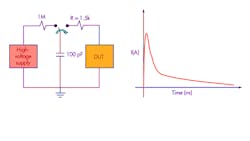
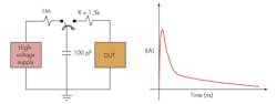
For HBM tests, there is a simple series RC network to simulate the discharge from a human body. A 1-MΩ resistor is used to charge a 100-pF capacitor. A 1.5-kΩ resistor is used for discharging. HBM events are most disruptive with fast rise times. Therefore, fast rise time pulses are required to more precisely simulate a HBM discharge event.
The discharge current, i(t), is defined by:
i(t) = i0 exp(–t/τ)
where:
i0 = VHBM/(RDUT + R)
and:
t = C(R + RDUT)
R = 1.5 kΩ
Power dissipation to the device under test (DUT) is:
P(t)=i2(t) RDUT
Total energy delivered to the DUT is:
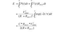
The heat generated depends upon the capacitance, DUT resistance, and peak voltage of the ESD pulse. In HBM testing, IC failure modes typically show gate oxide, contact spike, and junction damage. Figure 1 shows test setup and current waveform characteristics. A high voltage is applied in series with a 1-MΩ resistor and a 100-pF capacitor. After the capacitor is fully charged, it’s discharged to the DUT pin through the 1.5-kΩ resistor.
Charged Device Model
CDM simulates device damage that could not be simulated by HBM testing. It simulates a device charged either directly by triboelectric effect (see “Harvesting Power Using Triboelectric Generators”) or indirectly by electrostatic induction and static charge stored in a part’s body that discharges in an outside environment.
This test is used to simulate situations that happen in manufacturing environments such as mechanical device handling where devices slide down shipping tubes or test handlers that build up a charge that’s subsequently discharged to ground. Figure 2 shows the CDM ESD test and typical current waveform characteristic. When an external ground touches the DUT pin of the charged device, the stored charge will be discharged from the device to the outside ground. In the CDM test, the device is kept on its back, facing upward on a test fixture.
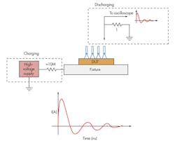
CDM currents are higher than HBM currents because there is no current limiting resistor in the path to limit the discharge. For a 500-V test voltage, the current waveform rise time is generally around 400 ps with the peak current around 6 A for 1.5 to 2 ns. For a 1000-V test voltage, the peak current magnitude is around 12 A.
Machine Model
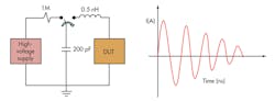
Also known as the 0-Ω model, MM is designed to simulate a machine discharging through a device to ground. Failure modes in MM testing are similar to those in HBM testing. In the test setup, a high-voltage (HV) supply in series with a resistor charges a capacitor. A switch is used to remove it from the HV supply and connect it to the inductor for discharging. The inductor produces an oscillatory current waveform.
MM uses the same basic test circuit as HBM, except R = 0 Ω and C = 200 pF (Fig. 3). A 200-pF capacitor, which represents a conductive object such as a metallic handler, is used with a 1-MΩ resistor for charging. A 0.5-μH inductor is used for discharging. The MM test is less commonly used than the HBM test. The MM current characteristic waveform consists of both positive and negative sinusoidal peaks that decay exponentially.
Model Comparison
Similar rise times (i.e., ~10 ns) and total duration for HBM and MM cause comparable joule heating that results in similar failure mechanisms for both models. The failure signature and discharge processes of the MM test are generally the same as that of the HBM test. Thus, the HBM test could guarantee MM ESD robustness.
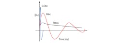
Usually, the stress level of MM ESD is approximately 10 times lower than that of HBM ESD. Also, the protection voltage level for HBM typically is ~2 kV while for MM it is ~200 V and for CDM it is ~500 V. CDM is completely different from HBM and MM, so there is no correlation between them. Therefore, CDM and HBM tests are commonly used to test ESD protection circuits. Figure 4 shows current waveforms characteristics for HBM, MM, and CDM. The CDM waveform corresponds to the shortest known ESD event and has a rise time of 400 ps with a total duration of ~2 ns.
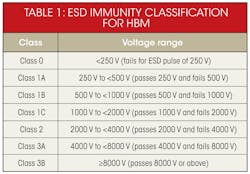
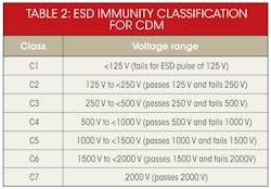
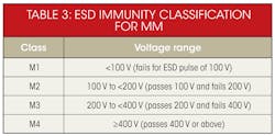
Classification Of ESD Immunity
The ESD sensitivity of a device can be defined as the highest ESD test voltage it passes and the lowest ESD test voltage it fails. Each model has its own classification for categorizing devices according to their ESD sensitivity (see the tables).
Sanjay Agarwal is a senior product engineer working in timing solutions at Cypress Semiconductor, Bangalore. He holds a master of technology degree from the Indian Institute of Technology Kanpur, specializing in electronic materials, device fabrication, and characterization. He has authored numerous technical articles for semiconductor electronics publications.
About the Author
Sanjay Agarwal
Sr. Product Engineer
Mr. Sanjay Agarwal is working as Sr. Product Engineer in Timing Solution, Cypress Semiconductor, Bangalore. Mr. Sanjay Agarwal holds a Master of Technology degree from Indian Institute of Technology Kanpur specialized in Electronic Materials, device fabrication and characterization. He has authored numerous technical articles in semiconductor electronics publications.
Comment About the Article
To join the conversation, and become an exclusive member of Electronic Design, create an account today!

Leaders relevant to this article: