GaN Ups Efficiency in Next-Generation Wireless Chargers
Shipments of wireless-charging base stations are expected to pass 500 million annually in the next few years according to IHS Markit. This growth is driven by expanding numbers of consumer electronics devices that support or rely exclusively on wireless power for battery renewal.
Not surprisingly, engineers designing chargers are seeking a competitive edge in building devices that produce higher efficiency, a smaller footprint, and lower system cost. Substituting gallium-nitride (GaN) e-mode high-electron-mobility transistor (HEMT) devices for traditional MOSFETs in class D and class E amplifier technologies is a viable route to achieve these goals.
Wireless Charging Overview
Wireless chargers are similar to wired charging in that both are switched-mode power-supply (SMPS) designs. In the wireless system, the magnetically coupled transformer element of the design is split between a transmitter unit (the charger) and a receiver (target device). Multiple receivers with different power requirements may be able to use the same transmitter.
Today’s most widely used wireless-charging techniques utilize inductive coupling, operating in the 100- to 300-kHz frequency range. Induction performs well for near-contact charging of single devices and can be configured with multiple coils to achieve some degree of positioning flexibility. This also makes it possible to charge several devices within about 10 mm of vertical freedom.
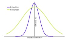
Moving from inductive to magnetic-resonance transmitters operating at high frequency (6.78 MHz as defined by the AirFuel Alliance) expands the reach of the charging field up to 50 mm, enabling more flexibility to charge several devices at once and allowing for less restrictive physical orientation of the charging targets. Efficiency is higher in the “sweet spot” of an inductive device, but the resonant device has a wider range where it can efficiently charge devices (Fig. 1). This enables a “drop and go” charge experience, instead of requiring users to pay close attention to how they place a device.
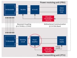
Two-part wireless-charger systems consist of a transmitter unit connected to a power source and a receiving unit integrated into the end-user device (Fig. 2). Infineon, a provider of all types of power transistors and the MCUs used in such designs, evaluated how GaN power transistors would affect the performance of this type of system.
We know that the figures of merit (FOM) of GaN devices compared to best-in-class silicon-based MOSFETs indicate an improvement in performance of nearly an order of magnitude. The question was how this would translate to system designs using GaN e-mode HEMT devices in the power amplifier block of the power transmitter.
Performance versus MOSFETs
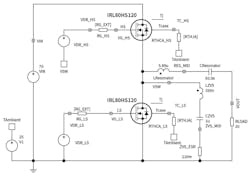
The evaluation used well-understood class D and class E power amplifier designs. A class D amplifier is similar in topology to a dc-ac inverter. Relatively high input voltages (50 to 100 V) are needed to transmit significant power, and the combination of high voltage and the 6.78-MHz frequency call for zero voltage switching (ZVS) turn-on. This is accomplished with an LC network to create a triangular-shaped current that’s higher than the load current (Fig. 3).
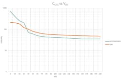
In this amplifier, the largest system-level loss contribution at more than 50% is dc resistance at the ZVS inductor and other instances in the ZVS path. Attention should be paid to the QOSS device parameter of the inductor to best manage these losses.
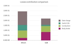
At the device level, the largest loss contribution comes from the gate charge (QG), so both lower gate charge and lower threshold devices are recommended. In addition, since ZVS isn’t achieved under all operating conditions, it’s important to consider the impact of some switching loss.
Considering all of these factors, the comparison of a class D topology and ZVS to a similar silicon-based amplifier design shows reduced power losses in the range of 30% (Fig. 4). Importantly, the device area of the required GaN transistors is half that of the equivalent MOSFETs, representing a doubling in power density.
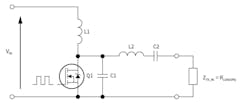
Single-ended class E power-amplifier topology is comprised of an RF inductor (L1) that supplies current to a switching FET (Q1), a resonant circuit, and load (Fig. 5). When properly tuned and with a controlled output current to limit power loss from conduction and eddy-current loss in L2, a GaN-based class E amplifier achieves significantly improved performance compared to the same circuit implemented with a silicon MOSFET.
A design rated up to 16 W was evaluated with a resistive load at 25 Ω, 15 Ω, and 5 Ω. The GaN device offered improved overall efficiency and was able to support a wider load-impedance range. The log scale comparison in Figure 6 shows the consistently higher output voltage at similar voltage levels achieved with GaN.
Best-Practice Design Considerations
Foremost among GaN benefits is the reduced gate-drive voltage requirement—just 5 V as opposed to the 10 V required for standard silicon MOSFETs. Gate charge for a GaN device is typically one-fifth that of MOSFETs, paving the way for overall reduction of losses related to the driver circuitry. However, the wide range of acceptable drive voltage for MOSFETs allows for relatively simple and low-cost voltage regulation.
Designs using GaN call for more exacting voltage-regulation design to prevent overcharge that might cause device failure or reduced operating lifetime. Similarly, gate-drive voltage must be tightly controlled, as leakage current through the Schottky barrier used for GaN designs may be in the range of milliamps instead of nanoamps.
As noted, GaN devices support a doubling of power density as a result of the low RDS(ON) × area figure compared to silicon MOSFETs. This potentially reduces the contact area of the device in relation to its PCB mounting and can affect power dissipation. Careful attention to PCB design to manage thermals can readily compensate for these effects.
In summary, GaN e-mode HEMT implementations can yield improved efficiency, smaller size, and lower-cost designs of wireless power transmission units when compared to silicon MOSFETs. The key to success is to recognize and take full advantage of the improved FOMs of GaN devices in power-amplifier design. With full attention, engineers can gain improvements of 30% or more while saving in other system cost elements by lowering cost of other components and reducing the total BOM.
For more information about GaN devices available from Infineon, click here.
Milko Paolucci is an Applications Engineer for Consumer and Industrial Wireless Charging at Infineon Technologies AG, and Peter Green is Applications Manager for Renewable Energy at Infineon Technologies Americas Corp.
About the Author
Milko Paolucci
Applications Engineer for Consumer and Industrial Wireless Charging, Infineon Technologies AG
Peter Green
LED Group Manager
Peter Green is the LED Group manager, energy saving products, at International Rectifier Corp. He received a BSc in electrical engineering from Queen Mary College, University of London, in 1985. Since then he has worked in product design and development for commercial and military companies in the power supply and lighting industries in the U.K. He is a member of the Institution of Engineering and Technology and a Chartered Engineer. In 2001 he relocated to California to join the Lighting Design Center at International Rectifier, where he has worked on new lighting ASIC definition and design, as well as application support. He is currently managing LED systems and applications. He has previously presented at APEC, PCIM, and many other conferences and has several patents related to lighting electronics. He can be reached at [email protected].
Voice Your Opinion!
To join the conversation, and become an exclusive member of Electronic Design, create an account today!

Leaders relevant to this article:
