
Download this article in PDF format.
The dc-dc converter has become a standard part of many designs simply because there are many different configurations that address almost any need. Two of the toughest applications for dc-dc converters involve electrical circuit isolation and high-voltage generation. Now, you can take on those challenges easily with some interesting new dc-dc converter ICs.
Sponsored Resources:
- Power Through the Isolation Barrier: The Landscape of Isolated DC/DC Bias Power Supplies
- Designing Bipolar High Voltage SEPIC Supply for Ultrasound Smart Probe
- How to find the right isolation solution for your application
Transformers: Still the Best Way to Provide Electrical Isolation
When it comes to designing circuits that require electrical isolation, you probably know or should know that there’s probably nothing better than a transformer to provide it. Separate windings easily pass signals magnetically from primary to secondary. With this form of energy transfer, the primary circuit is electrically isolated from the secondary circuit. The insulated windings block dc and make it possible to have separate grounds.
A transformer isolation barrier is a good design choice, but you still must find the right transformer. Even worse is having to design that transformer yourself, if you can. For isolation involving the 60-Hz power line, your only real choice is a big, heavy transformer. The good news is that for many applications, you can use an integrated-circuit transformer. Figure 1 shows a transformer that’s fully contained within an integrated circuit along with a dc-dc converter.

Here are just a few examples of applications that typically require some form of electrical isolation:
- DC bias supplies
- Analog input and output modules for PLCs
- Voltage and current sensing
- Smart breakers and protection relays
- RS-485 and CAN buses
- Patient monitoring
- Where you must supply dc that has been isolated
- Use cases where you need to keep high-voltage (HV) circuits away from low-voltage circuits or you need to help prevent electrical shock.
You will find a good introduction to this subject in the TI App Note “Power Through the Isolation Barrier: The Landscape of Isolated DC/DC Bias Power Supplies.”
Isolation Primer
There are several types of isolation—your application will identify the type you need. It’s often dictated by the safety standards that you may have to meet, such as those of the International Electrotechnical Commission (IEC). Here’s a quickie summary of the four basic types:
- Functional isolation: Plain old electrical isolation. No shock protection.
- Basic isolation: Same as functional isolation but adds the shock protection.
- Double isolation: This is basic isolation plus an additional layer of shock reduction.
- Reinforced isolation: A variation of double isolation with added safety measures.
Which one do you need? Learn more from this instructional blog. It further defines the four major types of isolation and explains how you can benefit from TI’s new fully integrated transformer technology, which delivers several advantages compared to other reinforced isolation solutions.
Chip Solutions
What are these magical devices that provide this superior isolation? They are the TI UCC12050 and UCC12040. The UCC12050 isn’t only just a dc-dc converter IC but also has an internal isolation transformer. It’s designed for a dc input in the 4.5- to 5.5-V range and can deliver an output of 5 or 3.3 V with a selectable 400-mV headroom adjustment to accommodate an external low-dropout regulator (LDO). Output power is 500 mW.
Some additional features include short-circuit recovery, thermal shutdown, and an extended temperature range: −40 to +125°C. The package is a 16-pin wide-body SOIC with >8-mm creepage and clearance.
Isolation rating details include 3 kV for the UCC12040 and 5 kV for the UCC12050. The working voltage is 800 V and 1.2 kV for the UCC12040 and UCC12050, respectively; however, the surge ratings are 8 kV and 10 kV for the UCC12040 and UCC12050, respectively. The UCC12050 also complies with a wide range of safety measures that meet various regulations or certification guidelines.
Figure 2 shows a typical application. The 4.5- to 5.5-V input is applied to the EN pin. Bypass capacitors of 10 µF and 0.1 µF are recommended for both input and output. The output voltage is set with the resistor RSEL on the SEL and VISO pins. Output choices are 5.0, 5.4, 3.3, and 3.7 V.
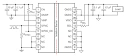
SYNC is an input for an external clock if you want to synchronize multiple similar devices. SYNC_OK detects and selects whether an external clock is used. The internal clock is 8 MHz. Now you can understand how to integrate the transformer.
If you’re searching for an isolation device, the UCC12050 is worth a look. An evaluation module (UCC12050EVM-022) is available to help you determine if the UCC12050 fits your application.
Designing a High-Voltage Power Supply for an Ultrasound Probe
One product that needs a high-voltage supply is an ultrasound imager. Ultrasound has become a widely used medical imaging diagnostic tool. The usual configuration is a large cart-based console with a display and a cable-connected probe. The trend is to put all of the electronics in a handheld probe. The design challenge, though, involves a dual high-voltage dc supply that must generate very low noise but be highly efficient.
The two usual choices for HV switching-supply topologies are flyback and SEPIC. The flyback arrangement uses a step-up transformer to provide the HV. A custom transformer is usually needed, however, making it a secondary choice.
HV can also be provided by the SEPIC (single-ended primary-inductor converter) topology in a boost configuration. The SEPIC configuration was chosen for this design because it works with very low input voltages, doesn’t require a transformer, uses off-the-shelf inductors, generates less noise than other topologies, and is very efficient. The output-voltage boost comes from the use of several inductors.
Figure 3 shows the basic SEPIC configuration. It uses two parallel inductor-diode circuits that provide the dual ±80 V outputs. The low-voltage input is controlled by the input inductor L1 and a MOSFET switch driven by a PWM signal. As the MOSFET switches, the inductors and capacitors exchange energy as the input voltage is stepped up and delivered to the load. Even with a low battery input voltage, the circuit can be designed to produce an output up to ±100 V.
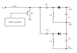
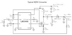
Figure 4 shows a practical implementation of this configuration. It uses a TI LM3488-Q1 boost dc-dc converter that supports SEPIC or flyback configurations. This tiny (3 × 3 mm) device can accept a dc input ranging from 2.97 to 40 V. It switches at a frequency between 100 kHz and 1 MHz as set by an external resistor. Only one HV output is shown. To achieve the dual ±80-V outputs required by the probe, add another output to the drain of the MOSFET similar to the circuit with C5, L2 , COUT, and the diode.
Check out the application report “Designing Bipolar High Voltage SEPIC Supply for Ultrasound Smart Probe.” It provides a solution to generate programmable output voltages of up to ±100 V by introducing an intermediate boost stage.
Sponsored Resources: