
Use Laser-Flash Thermal Conduction Measurements to Evaluate Power-Semi Packaging Materials
Download this article in PDF format.
The power-semiconductor industry is experiencing growth exceeding 7% per year, driven by new applications such as electric cars and new technologies like silicon-carbide (SiC) and gallium-nitride devices. These new applications and technologies put increasing demands on power-semiconductor package performance. Specifically, power-semiconductor packaging technology must address key requirements:
- Ability to conduct the large electrical currents that flow through the device and package.
- Need to provide an effective thermal path between the device and heat sink to keep the device junction temperature within specification.
- Ability to withstand temperature and power cycling (and the resulting CTE stress) without mechanical damage, including dielectric cracking or metal delamination.
The requirement to channel very high electrical current narrows the potential metallization systems down to the best conductors: silver (Ag), copper (Cu), or aluminum (Al). Of these, thick Cu and Al are more favorable due to higher resistance to electromigration compared to Ag.
The thermal requirements, which will be the major focus of this article, requires metallization with high thermal conductivity, dielectric materials with high thermal conductivity, and low interfacial thermal impedance at the metal/dielectric interface. For this reason, the dielectrics of choice have been AlN (thermal conductivity > 170 W/m-K), Al2O3 (thermal conductivity = 25 W/m-K), and Si3N4 (thermal conductivity of 67 W/m-K).
The ability to withstand temperature or power cycling has been one of the largest challenges for power-semiconductor packaging technology. The combination of metals that have very high thermal expansion (Cu CTE = 17 ppm/°C) with dielectrics that have very low thermal expansion (AlN = 4.5 ppm/°C) leads to very large thermal expansion stress during temperature cycling. This is particularly the case at low temperatures, where a large tensile stress develops at the edges of the metallization.
Such high tensile stress can result in dielectric cracking. For this reason, very high flexural strength ceramics like Si3N4 are increasingly being utilized for the highest power applications where the temperature cycling stresses are the largest.
The focus of this article will be to provide a quantitative evaluation of the thermal resistance between the metallization system and the dielectric by utilizing a laser-flash technique. The thermal resistance of this interface will directly impact heat conduction through the package since this interface is located between the die and the heat sink. A schematic of the thermal path for a packaged power semiconductor is shown in Figure 1.
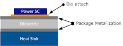
1. Shown is a schematic of a packaged power semiconductor illustrating the heat path from the die, through the package to the heat sink.
Laser-Flash Thermal Conduction Measurements—Applied to Layered Structures
The laser flash technique described here follows ASTM E 1461. In this measurement, a short laser pulse illuminates the front surface of the sample, creating a heat pulse. The subsequent temperature rise is measured on the back surface of the ceramic using a sensitive infrared detector. The overall temperature rise is typically only a few degrees centigrade. The temperature rise on the back surface as a function of time is fitted to a one-dimensional heat flow model and the thermal diffusivity of the sample is determined.
Thermal conductivity is the product of the sample density, heat capacity, and the measured thermal diffusivity. A typical temperature rise profile measured on the sample backside as a function of time is shown in Figure 2.
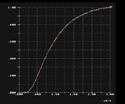
2. The temperature rise on the backside of a thermal conductivity sample is shown as a function of time in the laser-flash measurement system.
The time = 0 for this profile begins when the laser pulse is incident on the sample. Figure 3 depicts a schematic of the laser-flash system used for these measurements.
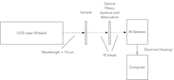
3. Schematic of the Laser Flash Thermal Conductivity Measurement System.
In our laser-flash system, a pulsed CO2 laser with a wavelength of 10 µm and 5-µs pulse duration was used to illuminate the front side of the sample. A liquid-nitrogen-cooled HgCdTe IR detector was used to measure the temperature on the backside of the sample.
For a monolithic sample, this temperature rise is fitted to a 1D heat flow model; the thermal diffusivity of the sample is determined from this fit. The time-dependent temperature of the backside of the sample T(t) in the 1D heat from the model is described by:

where t is time after the laser pulse, T(0) is the initial backside temperature at t=0, Tm is the maximum backside temperature after the laser pulse, L is the sample thickness, and a is the thermal diffusivity.
If we input the experimentally measured time required for the sample backside to reach 0.5 Tm, t1/2, then from the equation above, calculate the thermal diffusivity:

The thermal conductivity is the product of the thermal diffusivity a, sample density (r), and heat capacity cp.
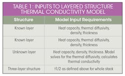
The discussion above is relevant for monolithic samples. However, the laser-flash technique can also be applied to layered structures. In this case, a model is utilized which considers one dimensional heat flow through a layered structure. Application of the diffusion equation to layered structures is discussed in Reference 1 and references therein. The input requirements for a three-layer model are shown in Table 1.
This measurement is very useful for evaluating thermal resistance in “real-world” situations since the “unknown layer” comprises the layer itself and the interfaces between the “unknown” and known layers.
Here, we will utilize this approach to quantify the thermal resistance between the metallization systems relevant to power-semiconductor packaging and the ceramic dielectric layers. We will consider the three cases described in Table 2.

Samples Evaluated
The DBC sample that was measured came from a commercial DBC vendor. The active Cu samples were prepared from commercial ABA Cu alloy foils that were brazed in an argon atmosphere at 1025°C to AlN, Si3N4 substrates and to OFC Cu foil. In addition to the sandwich structure samples (with ABA in the middle layer), a sample was constructed with Si3N4 dielectric bonded to ABA Cu, which was bonded to Cu foil.
Argon was chosen to avoid any interaction between the Ti, Al, and Si in the ABA Cu foil and the furnace atmosphere. All samples were x-rayed to ensure that there were no voids at the braze joints.
Laser-Flash Measurement Results
The thermal conductivity of the ABA foil as a 50-µm-thick free-standing foil was also measured. The thermal conductivity was found to be 35 W/m-K.
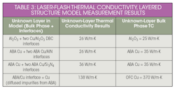
The results of the laser-flash thermal conductivity measurement and layered structure model for the packaging systems outlined in Table 2 are summarized in Table 3.
Key observations from these measurements include:
- For both the DBC samples and the ABA Si3N4 samples, the interfacial thermal impedance was negligible. This indicates an intimate, chemically bonded interface between the Al2O3 and Cu in DBC, and between the ABA Cu and Si3N4 in the ABA copper samples. The microstructure of these interfaces will be explored in the next section.
- The interfacial thermal impedance of the ABA Cu/AlN interfaces decreased the effective thermal conductivity of the layer from 35 W/m-K to 26 W/m-K.
- When ABA Cu is used to bond Cu foil to Si3N4, the conductivity of the Cu layer is greatly reduced, from close to 380 W/m-K for OFC Cu to only 138 W/m-K. The reason for this reduction is discussed below.
Microstructures
All of the samples discussed above were cross-sectioned with an ion mill and then imaged on a high-resolution SEM.
In Figure 4, the interface between the Al2O3 and Cu with the DBC bond is shown at 10,000X and in Figure 5 shows a high-resolution image at 160,000X. It’s clear from this figure that the Cu/CuO interfacial layer in DBC is extremely thin, less than 90 A.
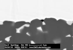
4. This is an SEM image of the Cu/Al2O3 interface in the DBC sample.
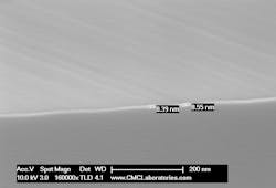
5. This is a high-resolution SEM image of the Al2O3/Cu interface in DBC.
Figure 6 shows an ion-mill cross-section for ABA Cu on Si3N4. In this case, the interfacial phases are much thicker, on the order of 1 µm.
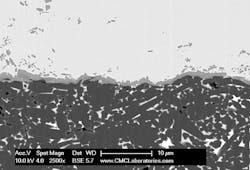
6. Ion-mill SEM cross-section of ABA Cu on Si3N4.
Figure 7 shows the phase composition of the interfacial layer taken from EDS mapping through the interface. This elemental mapping shows the presence of two interfacial layers: Ti-Al-Cu-N phase and a Ti-Si phase. Even with the presence of these intermetallic layers, the laser-flash measurement indicates minimal impact on heat flow.
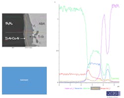
7. This elemental map was taken in an SEM with EDS of the ABA Cu/Si3N4 interfacial phases.
Figure 8 illustrates an EDS analysis in the SEM of the interface between the ABA Cu layer and the AlN ceramic. In this case, a distinct Cu-Ti-N layer that’s about 2 µm thick has formed. The laser-flash measurements indicate that this interfacial layer has a measurable impact on the overall thermal impedance of the structure, decreasing the effective thermal conductivity from 35 to 26 W/m-K.
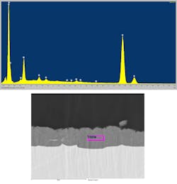
8. An elemental analysis was taken in an SEM with EDS of the ABA Cu/AlN interface.
For the Si3N4/ABA Cu/Cu sample, the composition of the Cu layer was analyzed with EDS as a function of the distance from the ABA interface (Fig. 9). The ABA layer was 50 µm thick and the Cu was 250 µm. As can be seen in Figure 9, Al had diffused more than 200 microns into the Cu layer during the fabrication process, and Si had diffused more than 150 microns into the Cu (the “0” point in this figure is the ABA/Cu interface).
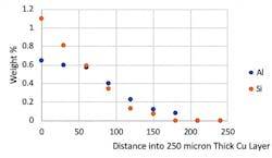
9. Al and Si impurity concentration is plotted as a function of distance from the ABA Cu/Cu interface into the Cu layer.
The presence of the Si and Al impurities in the Cu layer greatly decreases the layer’s thermal conductivity. The Cu thermal conductivity drops from 380 W/m-K, typical of pure Cu, to only 138 W/m-K.
The significant impact of the thermal conductivity of Cu on impurities, as observed here, is due to electron-impurity scattering, since heat is carried in metals by conduction electrons. This impact can also be seen in electrical conductivity (Fig. 10). In this case, the change in Cu resistivity for additions of various impurities (including Al and Si) is shown. Note that both heat and electrical current in metals is carried by electrons; therefore, both properties are impacted by electron-impurity scattering.
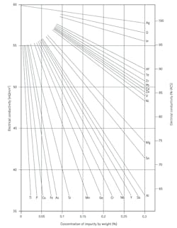
10. This figure (taken from Reference 2) shows Cu electrical conductivity with various impurity additions.
Conclusions
Laser-flash thermal conductivity evaluations of ABA Cu on Si3N4 as well as ALN ceramics has been performed, in addition to evaluation of DBC Cu on Al2O3. Bulk thermal conductivities of the ABA Cu, alumina, ALN, and Si3N4 were measured. In addition, the thermal diffusion time through the layered structures were also determined and a model was utilized to determine the interfacial thermal resistances in each system. The following findings resulted from this study:
- For the Si3N4/ABA Cu and Al2O3/DBC Cu, no significant thermal impedances were measured. In other words, there was no hindrance of heat flow through the interface structures even though intermetallic layers formed.
- The AlN/ABA Cu interface did have a modest impact on the overall thermal impedance of the layer, lowering the effective thermal conductivity from 35 W/m-K to 26 W/m-K.
- The thermal conductivity of the ABA Cu was about 1 order of magnitude lower than pure Cu with a thermal conductivity of 35 W/m-K. This layer does represent a hindrance to heat flow compared to a pure Cu layer. Consequently, making the ABA bonding layer as thin as possible would be advantageous.
- For DBC, there’s no significant thermal impedance. The interfacial layer between the DBC Cu and alumina was extremely thin, only about 8 nm.
- For both ABA Cu on AlN and Si3N4, intermetallic nitride layers were observed between the ABA Cu and the ceramic. For the Si3N4 sample, this intermetallic had no impact on heat flow. For the AlN sample, there was a measurable, but modest, impact.
- When ABA Cu is used to bond a pure Cu layer to Si3N4, diffusion of Al and Si into the pure Cu greatly reduces the Cu thermal conductivity, from above 380 W/m-K to 138 W/m-K. Consequently, a significant amount of the advantage that’s gained by using Cu in this application is lost due to impurity diffusion. Note that this effect is due to the impurity diffusion from the ABA into the Cu and isn’t related to the Si3N4.
Dr. Jonathan Harris is President, Erich Rubel is Director of Analytical Services, Rutilio Olivar is Director of Business Development and Senior Failure Analysis Engineer, and Gabe Carrasco is Senior Test and Design Engineer at CMC Laboratories Inc.
References
1. H.Y. Lee and R.E. Taylor, “Determination of Thermophysical Properties of Layer Composites by Laser Flash,” in Thermal Conductivity 14, (P. Klemens and T.K. Chu, eds.), Plenum Press, NY. pp 423-434 (1976).
2. David Chapman, High Conductivity Copper for Electrical Engineering, Copper Development Association Publication No 122, European Copper Institute Publication no Cu0232, February 2016.