Are Quantum-Tunnel Transistors Real, and What Do They Mean for Power Tech?
It's difficult to take the audacious claims being made by Search For The Next (SFN), a Nottingham, England-based technology startup, seriously. That’s because, if they are true, it will force the entire semiconductor industry to question the assumptions on which we've based nearly everything for the past 50+ years. Then again, after even a brief introduction to their research, and how they intend to apply it, it's even more difficult to ignore them.
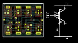
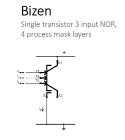
SFN says that its new process, referred to as “Bizen,” is based on the principles of quantum-tunnel mechanics, and can be used to dramatically improve the performance and producibility of any digital or analog semiconductor device. Among other things, making Bizen devices requires half the process layers, which cuts the 15 weeks it takes to process a typical wafer full of CMOS devices to just three weeks. In addition, SFN says that the new process achieves a three-fold increase in gate density that produces a matching three-fold reduction in die size.
In a recent announcement, SFN said that it has been collaborating with Semefab, a privately owned semiconductor and MEMS fab based in Glenrothes, Scotland, since 2017 on process development and qualification that should lead to device production in the near future.
David Summerland, CEO of SFN, explains, “The CMOS processing industry is hitting a brick wall as shrinking geometries bash up against the laws of physics. We went back to the very beginning and found a way to commercialize quantum-tunnel mechanics in silicon or wide-bandgap device manufacture. The result is ‘Bizen’—Bipolar/Zener—which retains the advantages of traditional bipolar processing yet removes the disadvantages by using Zener quantum-tunnel mechanics.
“This results in lower dynamic power, higher speed, and higher gate density, halving the number of process layers required, reducing material use by two-thirds, and slashing manufacturing time. This allows any fab, such as Semefab (Si), Plessey (GaN), or Newport (Compound), to become a category killer.”
Bizen vs. Bipolar
Summerland contrasted Bizen to bipolar technology, which has traditionally been limited by its requirement for bulky monolithic resistors that eat up silicon real estate and power. On the other hand, a Bizen transistor uses quantum-tunnel technology, which eliminates the resistor (as with MOS devices) and allows designers to take advantage of the now-controllable current. This enables the realization of a very low power circuit in which the transistor is "Normally On" but not saturated, and is controlled by an isolated tunnel connection rather than a direct metal contact to the base well, as used in traditional bipolar transistors.
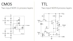
In addition, it’s expected that the simpler structure enabled by Bizen technology will allow designers to create a simpler circuit with far fewer layers and increased logic density. For example, the number of layers needed for a Bizen device range from four to eight for devices that support low- to high-voltage operation, compared with 10 to 17 for CMOS. In addition to smaller size and faster production cycles, Bizen devices are supposed to enjoy significantly reduced power consumption and faster operating speeds. Thus, complex devices can be manufactured in the large geometry fabs that exist in the U.K.
If the claims made by Allan James, Semefab’s CEO, prove to be correct, the power community may be looking at a radical shift in how we design products, and what we believe is possible. James says, “Semefab engaged with SFN, exploring ways to reduce smart power IC process complexity whilst retaining an ability to program the chip. Early suggestions were rejected because they could not meet the low mask count target required to be disruptive in the industry. Eventually, SFN hit on the idea of using the quantum-tunnel effect of miniature, reverse-biased Zener diode structures. It transpired that the integration of conventional lateral and vertical bipolar structures can, with careful modeling, be designed to incorporate Bizen without undue additional process complexity.
“I was initially quite skeptical but having lived with the concept and seen early-stage results, it does indeed tick many of the boxes needed to disrupt the industry,” he continues. “It's not so much a question that CMOS is flawed—although CMOS is prone to latch-up and ESD. CMOS is low power, has passed the test of time, and is generally reliable. However, it is complex and when integrated with power, even more so. Complexity means longer lead times and higher cost.”
James concludes, “If Bizen had been discovered back in the late 60s when the transition from bipolar to MOS and CMOS took place in order to cost-effectively integrate logic functions, it is possible that the industry may have developed strongly in the direction we are now proposing. It is not too late, however, and if it can be adopted by the industry, an important prize given the reduction in die area at a given technology node (comparing a Bizen and CMOS logic implementation) would be the ability to wind back the Moore’s Law clock by 10 years or more and bring many wafer fabs back into mainstream manufacture. There is still a way to go before Bizen becomes a commercial reality and we are still learning, however Semefab and SFN are working flat out to make it the huge success it may soon become.”
It's still too early to tell whether SFN's announcement is a promising, but ultimately fruitless development, or the beginning of a second semiconductor revolution. Whichever it is, I'll be working on some original reporting to keep you on top of the situation. Stay tuned…


