Download this article in PDF format.
Power density is a topic that most engineers are likely familiar with, but often don’t give it much thought. Or perhaps the thinking is that it doesn’t concern you. For your awareness, this article presents a general introduction on the subject, which seems to be a growing issue in electronic product design.
Sponsored Resources:
- Understanding the trade-offs and technologies to increase power density
- Understanding the fundamental technologies of power density
- Introduction to the fundamental technologies of power density
Defining Power Density
Power density is a term that more or less defines itself. For a more formal definition consider this: Power density is a measure of the amount of output power of a circuit or device divided by the volume of the device or product. The power value should be the continuous maximum amount of power the circuit can furnish under worst-case environmental conditions.
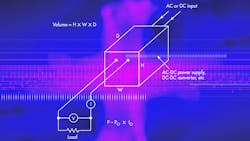
If you assume a rectangular package as shown in the figure below, volume would be the product of the height, width, and depth of the power source. Therefore, the power density (PD) would be:
PD = VoIo/(H x W x D)
Power density is generally associated with power supplies, power ICs, or any circuit generating power. For purposes of this article, we will use the power-supply reference for calculating PD.

One unit of measurement for PD is watts per cubic meter (W/m3) or watts per cubic inch (W/in3). Another related measure is current density or amperes per cubic millimeter or cubic inch (A/mm3 or A/in3).
Why Power Density?
Power density is important because of these factors:
- Smaller is better: The trend in all products over the years has been to make them smaller but still be able to do the same thing and put out as much as if not more power.
- Comparison factor: The power-density value gives you a direct way to compare switch-mode power supplies (SMPS) or almost any power product (dc-dc converters, audio power amplifiers, etc.)
- Power-supply volume is generally a concern in any new product: This is primarily because thermal considerations are so critical.
- Efficiency is a major issue concerning all electronics: Improving efficiency in power supplies also generally improves power density.
Achieving Power Density
One straightforward way to increase power density is to reduce component sizes. Choose the smallest possible capacitors, inductors, transformers and heat sinks required by the design. However, that technique has a limit because size is a major factor in the actual component value.
Such an approach can be pursued further if you’re able to increase the switching frequency. Switching regulators, dc-dc converters, and other switch-mode circuits don’t require as much filtering or energy storage at higher frequencies to achieve the same result. And significant size reductions in capacitors and inductors are possible at higher frequencies.
Early SMPS operated at less than 100 kHz. Newer designs moved into the 100 kHz and higher range. Today, most switching circuits operate at frequencies in the 1- to 4-MHz range.
While major size reductions take place at higher frequencies, there’s a limit to pushing those reductions further. That’s because continued increases in switching frequency escalates switching losses. This loss is mostly related to the switching transistor’s on-resistance or drain-source resistance (RDS(on)).
Lowering the on-resistance usually elevates gate charge and parasitic capacitances. Charging and discharging those parasitic capacitances of the transistor gates and drains takes some energy that increases overall losses.
One more factor that limits a boost in power density is reverse-recovery loss in the body diode of the main switching MOSFETs. Parasitic inductances also cause switching losses. Keeping the switching frequency down helps minimize all of these losses. The tradeoff, though, is balancing losses with smaller component sizes, making switching frequency a critical design factor. The choice of a power MOSFET for SMPS design is critical since various characteristics like RDS(on), the parasitic capacitances, die area, and switching frequency are closely tied together.
Power density is also impacted by the transistors’ thermal performance, which is a function of the increased switching losses. Getting rid of the heat—a major issue in SMPS design—is determined primarily by the packaging of the transistors or ICs.
Increasing switching frequencies has led to significantly reduced transistor and IC sizes, which has had a considerable effect on package design. The smaller the package, the more difficult it is for the device to dissipate its heat. In general, containing switching losses improves thermal performance. Innovative package design can improve heat dissipation and produce higher power density.
GaN Transistors
One sure way to achieve a desired level of power density is to use improved transistors or ICs. Those made with gallium nitride (GaN) perform particularly well in SMPS duty. These devices can operate at much higher frequencies with little or no reduction in efficiency. GaN device losses are much less than those of silicon or even SiC devices, allowing them to operate at much higher frequencies.
Combining GaN devices with innovative packaging will substantially increase power density. One such example is Texas Instruments’ HotRod QFN package. It reduces the parasitic inductances associated with more traditional packaging. An additional key to better heat reduction involves the bumps on some wafer chip-scale packages (WCSP)—they transfer most of the heat to the printed circuit board (PCB) for faster spreading and dissipating of the heat faster.
Additional gains in power density are the result of innovative designs, such as improved gate drivers and new converter topologies. One of the biggest gains comes from increased circuit integration. Putting more components and circuits in a small package significantly enhances power density.
One such example is to integrate the gate-driver circuit into the GaN FET package. By developing multichip modules with two or more die per package, power density will rise. Putting passive components inside the IC package is another integration method that produces fewer parasitics and reduces EMI. Finally, 3D stacking of components will also produce desirable gains. While reducing the footprint of a power supply or converter PCB is helpful, don’t forget to consider available vertical space.
In conclusion, improvements in power density can be achieved by a balanced mix of techniques that include lowering switching losses, improving the thermal performance with better packaging, and increasing the amount of integration. By keeping the concept of power density in mind as you design your next power supply or power circuit, you will automatically achieve increased efficiency, cooler operation, and smaller size.
Sponsored Resources: