
This Week in PowerBites: Batteries Get Smart and Fuses Get Even Smarter
DAQ System Delivers ASIL-D Compliance for EV Battery-Management Systems

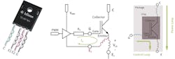
The MAX17852 14-channel, high-voltage, ASIL-D data-acquisition system from Maxim Integrated Products offers the highest level of safety for voltage, current, temperature, and communication, along with reduced space requirements and solution cost. Designed for integration within electric vehicles, hybrid electric vehicles, and other transportation systems, it can be used for smart junction boxes and automotive battery systems with voltages from 48 through 400 V—and beyond.
The MAX17852 is built with the precision and features that OEMs and EV manufacturers need to design their systems to meet the highest ASIL-D standards. The single-chip solution requires up to 16% less board space and 20% lower BOM cost than a discrete solution.
Thanks to its high measurement accuracy with tight time synchronization, the IC can measure cell voltage within ±0.45 mV at room temperature and a maximum of ±2-mV error across a temperature range of 5 to 40°C. In addition, with a current-sense amplifier range of ±300 mV, a maximum gain of 256, and maximum current-sense gain error of 0.3%, the MAX17852 provides fast, accurate data for calculating power management, state of health, and state of charge.
The 14-channel battery DAQ system integrates a current-sense amplifier to ensure current information is acquired synchronously with cell voltage and temperature. The MAX17852 allows both Hall-effect sensor and shunt resistors to be used as sensing components.
Availability and Pricing
- The MAX17852 is available at Maxim’s website for $7.52 (1000-up, FOB USA); also available from authorized distributors.
- The MAX17852EVKIT# evaluation kit is priced at $250.
- For details about Maxim’s BMS solutions, click here.
To order the MAX17852 or learn more, click here.
Resettable eFuse Includes Adjustable Overvoltage Protection Plus Flagging Capabilities

Toshiba Electronics Europe added the TCKE712BNL to its family of advanced eFuse ICs. Exhibiting a 53-mΩ on-resistance with a trip time of only 320 ns, the TCKE712BNL covers an input voltage range spanning from 4.4 to 13.2 V. This new device targets a broad spectrum of different consumer electronics goods, including cameras, cordless cleaners and power tools, cleaning robots, servers, smart speakers, thermostats, and wireless chargers.
eFuses are different from conventional glass tube and chip fuses, which provide one-shot protection against out-of-limit conditions. They’re designed to protect circuits during repeated over-limit events, after which they’re automatically reset by an internal logic signal. eFuses also have much faster responsiveness and can offer additional built-in protection functions.
For example, it’s possible to program the TCKE712BNL’s overvoltage threshold to fit with the specific application requirements. It also offers programmable overcurrent (also adjustable), overtemperature, and short-circuit protection mechanisms. And, unlike passive devices, it includes a flag function that transmits an external signal, which can be used to alert engineers of possible faults in the circuit design. The flag function also has a reverse-current blocking feature that allows the device to be employed in multiplexed systems.
The TCKE712BNL eFuse comes in a compact WSON10 package measuring 3.00 × 3.00 mm. For more information, visit the TCKE712BNL product page.
650-V "Hybrid" IGBTs Feature Co-Packaged Schottky Barrier Diode for Improved Efficiency

A new family of "Hybrid IGBTs" developed by Infineon Technologies combine key benefits of the company’s 650-V TRENCHSTOP 5 IGBT technology and the unipolar structure of a co-packaged Schottky barrier SiC diode. Members of the new CoolSiC product family offer superior switching frequencies and reduced switching losses, suiting them for dc-dc power converters and power-factor-correction (PFC) applications. This includes battery-charging infrastructure, energy-storage solutions, photovoltaic inverters, and uninterruptible power supplies (UPS), as well as server and telecom switched-mode power supplies (SMPS).
The Hybrid IGBTs can be used as drop-in replacements for TRENCHSTOP 5 IGBTs, allowing for an efficiency improvement of 0.1% for each 10-kHz switching frequency without redesign efforts. The co-packaged, freewheeling SiC Schottky diodes can switch rapidly without severe oscillations and risk of a parasitic turn-on, enabling them to deliver improved electromagnetic compatibility and system reliability.
For example, CoolSiC Hybrid IGBTs experience significantly reduced switching losses at almost unchanged dV/dt and di/dt values. They offer up to 60% reduction of Eon and 30% reduction of Eoff compared to a standard silicon diode solution. Alternatively, the switching frequency can be increased at least by 40% with unchanged output power requirements, thus making it possible to use smaller, lower-cost passive components.
The CoolSiC Hybrid discrete IGBT family comprises 40-, 50-, and 75-A, 650-V TRENCHSTOP 5 ultra-fast H5 IGBTs co-packaged with half-rated CoolSiC Gen 6 diodes, or medium-speed S5 IGBTs co-packaged with full-rated CoolSiC Gen 6 diodes. Designers can choose between a TO-247-3 or TO-247-4 pin Kelvin Emitter package. The fourth pin of the Kelvin Emitter package allows for an ultra-low inductance gate-emitter control loop and reduces total switching losses.
Additional information is available at www.infineon.com/coolsic-hybrid-discretes.
Low-Cost Sensors Enhance Energy-Meter Eval Board’s Accuracy, Galvanic Isolation
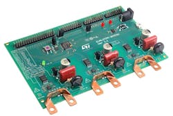
STMicroelectronics unveiled a new evaluation board intended to accelerate the design of cost-effective, three-phase ac wattmeters that meet the most stringent international standards for quality and accuracy. The reference design features low-cost, electromagnetic-immune shunt sensors and advanced galvanic-isolation technology for superior reliability and robustness. It can also be used as the basis for applications beyond utility metering, such as electric-vehicle charging, servers, and solar inverters.
The EVALSTPM-3PHISO evaluation board combines the STPMS2 high-accuracy metering front-end IC and the advanced STISO621 digital isolator, with customizable turnkey firmware running on an STM32 microcontroller to compute metrology and power-quality data. The sensing circuitry and PCB layout are optimized to ensure robustness against EMI and a strong signal-to-noise ratio for high-accuracy measurement and post-processing computation.
The STPMS2, is a two-channel, 24-bit, second-order sigma-delta modulator that measures voltage and current for each phase through an on-board voltage divider and a shunt-current sensor. It then oversamples the signal using a synchronized 4-MHz clock distributed by the microcontroller and multiplexes voltage and current sigma-delta bit streams on a single output pin. Three STPMS2s are used in the three-phase system to collect voltage and current data from each phase.
The multiplexed output from the STPMS2 is converted into 24-bit voltage and current values by the STM32 microcontroller, which uses its on-chip digital filters as sigma-delta modulators (DFSDMs). The processor then uses the resulting 24-bit voltage and current values to compute all necessary metrology data in real-time every 200 µs. The platform's firmware also implements a virtual com port that provides access to internal parameters for reading metrology data, modifying the internal configuration, and calibrating the board.
The STISO621 dual-channel digital isolator is the first in a new series of ICs that leverage ST’s 6-kV thick-oxide galvanic-isolation technology to transfer data between isolated domains in a variety of industrial applications. The STISO621 features two independent channels with Schmitt-trigger inputs that delivers high noise immunity and keep pulse distortion below 3 ns. With a maximum data rate of 100 Mbit/s, 6000-V impulse withstand voltage (VIOTM), and 1200-V maximum repeating isolation voltage (VIORM), the STISO621 ensures faster data transmission, longer lifetime, and higher reliability than conventional optical isolators.
ST’s metering evaluation board meets EN 50470-x, IEC 62053-2x, and ANSI12.2x standards for ac wattmeters. The application provides active wideband, active fundamental, reactive/apparent power and energy data, both per-phase and cumulative. Thus, it reaches accuracy Class 0.5 according to IEC 62053-22 on three-phase active/apparent power measurement and accuracy Class 1 according to IEC 62053-21 on three-phase reactive power measurement. It performs RMS and optional distortion (THD) calculations for each voltage and current signal, as well as dc measurements, and line period, phase shift, and phase-voltage delay for each phase.
The EVALSTPM-3PHISO also can be used as a reference for multi-phase industrial metering applications beyond utility metering like those mentioned above. Priced at $118, the EVALSTPM-3PHISO evaluation board is available now from st.com and distributors.
For additional information, visit www.st.com/isolated-interfaces
P-Channel MOSFETs Bring Superior On-Resistance, Withstand Voltages to 24-V Apps

ROHM Semiconductor's new 24-model family of 24-V input, −40/−60-V withstand voltage P-channel MOSFETs are available in both single and dual configurations. The devices are well-suited for industrial and consumer applications, such as factory automation, robotics, and air-conditioning systems.
The new MOSFETs use an advanced 5th-generation semiconductor process to achieve the lowest on-resistance per unit area in their class, according to the company. For the −40-V products, this translates to 62% lower on-resistance than conventional products, and 52% lower on-resistance for the −60-V products. They also employ an optimized device structure and new design that mitigates electric-field concentration, leading to high reliability and low on-resistance (which are typically in a tradeoff relationship). These solutions contribute to stable long-term operation in industrial equipment demanding exceptional quality.
The devices address the trend toward higher input voltages, driven by the growing need for higher efficiency in industrial and consumer applications. Although N-channel MOSFETs generally feature higher efficiency when used in the high side, a gate voltage higher than the input voltage is needed, complicating circuit configuration.
On the other hand, P-channel MOSFETs can be driven with a gate voltage lower than the input voltage, simplifying circuit configuration considerably while reducing design load. Applications include power-management switches and fan motors for industrial equipment.
All devices in this family are currently available in production volumes. Click here for additional information.
GaN Power ICs Target Consumer Apps with Easy Design-In and 66% More Power

The NV6128, a high-power 650-/800-V-rated GaNFast power IC, was developed by Navitas Semiconductor as a better alternative to the silicon-based devices currently serving the high-power mobile and consumer power electronics market. Housed in a 6- × 8-mm PQFN package featuring a proprietary, integrated cooling pad, the NV6128's lower 70-mW RDS(on) gives it a 66% increase in current capability. This suits it for high-efficiency, high- power-density 200- to 500-W applications such as all-in-one PCs, TVs, game consoles, eMobility chargers (eScooters, eBikes), gaming laptops, and more.
Like other members of the GaNFast power IC family, the NV6128 integrates a drive circuit, protection, and control to deliver the simplest, smallest power solution. It’s rated at 650 V for nominal operation plus a high, 800-V peak capability for robust operation during transient events. The GaN transistor's gate is fully protected and the entire device is protected against electrostatic-discharge (ESD) events of up to 2 kV.
“It provides a clear alternative to silicon-based power-conversion solutions,” said Dan Kinzer, Navitas CTO/COO and co-founder. “While some tier-1 OEM laptop adapters are still using traditional silicon-based diode rectification and boost PFC topologies that operate at 50 to 70 kHz, the GaNFast NV6128 enables a modern high-speed totem-pole architecture running at 200 kHz, enabling 300-W solutions at power densities of over 1.1 W/cc. And when you take full advantage of GaN's ability to support switching speeds in the MHz+ range, you get another major step-increase in power density.”
Design support includes detailed datasheets, electrical models (SPICE), and mechanical models (.stp). The NV6128 is in high-volume mass production and immediately available from Navitas distribution partners, priced at $7.85 at 1k units.
>> Electronic Design Resources
.. >> Library: Article Series
.. .. >> Article Series: PowerBites