How to Reduce the Number—and Size—of Output Capacitors in Power-Supply Designs
This article is part of TechXchange: Power Supply Design
Members can download this article in PDF format.
What you'll learn:
- What are output capacitors and how do they impact power supplies?
- Simulating a circuit to reduce the amount of capacitors in a supply.
- What is adaptive voltage positioning?
A power supply’s output capacitors—which are typically ceramic capacitors with values between 100 nF and 100 μF—cost money, take up space, and, in the case of delivery bottlenecks, can be difficult to obtain. Thus, the question of how the number and size of output capacitors can be minimized arises time and time again.
Output Capacitor Effects
Two effects of output capacitors are critical here: the effect on the output voltage ripple and the effect on the output voltage after load transients.
First, a general remark should be made about the term “output capacitor.” These capacitors can be found on the output of a power supply. However, many electrical loads (power consumers), such as FPGAs, require a certain number of input capacitors.
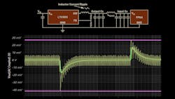
Figure 1 shows a typical design of a power supply with a load; here it’s an FPGA. If the physical distance between the voltage generation and the consumer on the circuit board is very small, the clear distinction between the power supply’s output capacitor and the input capacitor of the load becomes blurred.
Differentiation is usually achieved through a certain physical separation, which results in a significant parasitic inductance (Llayout).
The formation of capacitors at the output of a power supply determines the voltage ripple in a step-down (buck) switching regulator. The rule of thumb stating that the output ripple voltage corresponds to the inductor ripple current times the impedance of the output capacitors applies here:
VΔ = ILΔ × ZCout (1)
This impedance (ZCout) is made up of the size and number of capacitors as well as the equivalent series resistance (ESR) and equivalent series inductance (ESL). This formula is very easy to apply to one capacitor at the output of a power supply. For a more complex situation (Fig. 1, again) with multiple capacitors in parallel and series inductances occurring due to the layout (Llayout), the calculation isn’t as easy.
Applying LTspice
In this case, a simulation tool such as LTspice is ideal. Figure 2 shows a circuit diagram that was quickly created for the situation in Figure 1. Different values, including ESR and ESL, can be assigned to the individual capacitors. Assumed effects of the board layout—for example, Llayout—also can be considered. The voltage ripple is then simulated at the output of the switching regulator and at the input of the load.
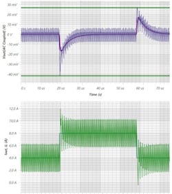
Output capacitors affect the output voltage offset after load transients, too. This effect also can be simulated with LTspice. Here, it should especially be noted that, within certain limits, the control speed of the power-supply control loop and the impedance of the output capacitors are interrelated. A faster power-supply control loop can decrease the number of output capacitors needed to remain within a specific output control window following load transients.
Adaptive Voltage Positioning
Last but not least, the LTC3311-1 has adaptive voltage positioning (AVP). AVP can utilize the entry error voltage budget and lower the number of output capacitors, on top of a reduction the designer may achieve, by increasing the loop bandwidth.
AVP raises the output voltage slightly in a low load condition and decreases the output voltage slightly during a high load condition. Then, if load transients occur, more of the dynamic-output-voltage deviation is within the allowed output-voltage range.
Using LTpowerCAD from Analog Devices is recommended when trying to find out which control-loop optimizations can be made and how many of the output capacitors can be eliminated. Figure 3 shows the screen for calculation of the control speed. The calculated voltage overshoot following a load transient is shown here. Optimization can be done by varying the output capacitors and adjusting the switching-regulator control-loop speed.
Read more articles in TechXchange: Power Supply Design


