Automotive Smart Fuse Aids in Diagnosing Intermittent Shorts (Part 2)
Members can download this article in PDF format.
What you’ll learn:
- How the smart fuse itself works, as opposed to a regular fuse, in a car.
- Operation details of the smart fuse’s power-on and bang-bang functionalities.
- How the smart fuse’s boot-up operation functions.
In the first part of this series, we examined the smart fuse and its functionality. Here we continue the explanation of how the fused current-pass transistors are selected and monitored via thermistors and the code algorithm to safely control the load current. We also will delve into how the smart fuse incorporates all required components of a formal data-acquisition system in order to understand the electrical current usage profile for the fused load that’s been causing pesky, intermittent shorts in my BMW.
Perhaps the nature of the current flow will clue us in as to where, exactly, the fault may lie…information we can glean from the smart fuse even when the intermittent short is NOT present.
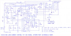
Again, we reference our smart-fuse schematic (Fig. 1). The actual current during normal operation (its usage profile) is unknown. It could be nominally at 3 A, having occasional peaks to 6 A, or it could be long periods at more than 5 A.
Either way, the current-pass elements, Q1 and Q3, must be rated to handle both the peak current amplitudes and the thermal requirements of long-period, high-current magnitude heating. It’s desirable to employ surface-mountable (vs. through-hole) FETs and be able to drive their gates directly (without level translators) by the GPIO outputs.
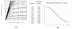
The Q1, Q3 VGS threshold at room temperature is ~2.5 V. Figure 2a shows the transfer curves for TK11S10N1L in a DPAK+ package, revealing that these devices’ channels can typically carry eight or so amps at VGS = 3.4 V. On-resistance (RDS(on)) is listed in the datasheet at 31 mΩ typical, 50 mΩ maximum at VGS = 4.5 V. Based on that, the RDS(on) is estimated at VGS = 3.4 V of ~ 40 mΩ at room temperature.
If the normal load current profile includes a constant 5 A for an extended period of time, the power dissipation of these transistors is IDS2 * RDS(on) ~= 25 * 0.04 = 1 W. That’ll get the package quite hot. but will probably be workable.
An increase to 6 A, however, will push that to 1.44 W, and without any real heatsinking or forced cooling will likely overheat the devices. In that case, different Toshiba N-channel FETs (e.g., TK33S10N1LLXHQ) in the same package can be used, although they’re 60% to 100% more expensive (and they’re not available now due to supply line shortages!). That’s why it’s convenient to pull the smart fuse into the controlled temperature ambience of the passenger compartment, as RDS(on) increases with temperature, which can be significantly higher under the hood.
Pass-Transistor Thermal Performance
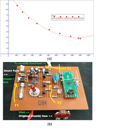
To measure the thermal performance of the pass transistors, thermistors are included as T1-T3. The first two have electrically insulating, grey thermal compound spread over their glass encapsulation, mating them to the Q1, Q3 drain tabs (Fig. 3). T3 measures the ambient temperature.
These thermistors must be rugged, reliable, and have good repeatability and reasonably high resistance value at room temperature so as to not draw too much power. The glass encapsulation makes for the ruggedness. Unfortunately, though, due to its associated mass and low thermal conductivity, it also makes for a lengthy overall thermal time constant (Tau) for the devices.
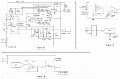
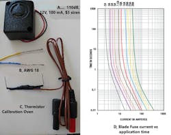
The thermistors are available on Amazon for about $0.17 apiece, compared to more than $0.40 each at the normal, go-to electronics distributors. Bundling them with other merchandise incurred $0 shipping costs. The downfall is that they’re delivered without a part number or datasheet, so, I put together the calibration oven (shown in Figure 10 part C, at end of article).
It consists of a double heat-shrink-wrapped package containing one thermistor (the leads are seen protruding downwards in Fig. 10); one 180-Ω, 2-W resistor (leads protruding upwards); and a Fluke type K thermocouple that plugs into any multimeter with a temperature setting. I pumped increments of 10 mA through the 180-Ω heater, waited for thermal equilibrium. and took thermistor resistance and associated temperature readings. The tabulated and graphical results are given in Figure 2b.
Figure 3 illustrates this same empirical data to a best fit polynomial curve, so we have the approximate R-T equation for the thermistors as:
R = 1.8 * T2 − 338 * T + 1.6733 * 104 (as would appear on the datasheet)
To calculate associated temperatures from thermistor resistance values as measured by the MCU’s ADC (shown in Figure 4, part C) and using integer math for faster computation, we have the following calculation:
T = (R2 * (71/64) – R * 18972 + 112,200,000) >> 20
I also measured T3’s thermal time constant in free air on the order of 7 seconds. Because there’s already a delay in real-time Q1, Q3 ADC temperature measurement due to Tau, it’s undesirable to include noise-filter capacitors (in parallel). That’s because it would only add delay to the real-time measurement and increase the difficulty of developing an effective algorithm.
Instead, it’s best to take the ADC measurements between bursts of the bang-bang to eliminate switching noise. The thermistors are only briefly energized via PF2 while these readings are taken to minimize system power consumption and thermistor self-heating.
Load Disconnect?
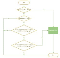
The algorithm is used to evaluate Q1, Q3 temperature performance and determine whether to disconnect the load to prevent overtemperature (Fig. 5). That algorithm is executed in the code whenever any of the following three conditions times out, as determined by the microcontroller’s cryotimer:
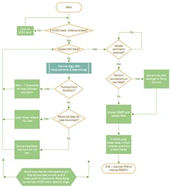
- Fault condition, which lasts for ~ 7.8 seconds and results in the load being disconnected either due to overcurrent from the intermittent short or overtemperature of either ambient, Q1 or Q3. The timeout here will be automatically repeated until the pass resistors significantly cool down after an overtemperature condition before attempted load reconnection.
- Ramping up the load current either just after boot or after a fault condition and subsequent cool-down period, if required. The full ramp takes place in ~ 0.1 seconds.
- Normal operation, which is interrupted every ~0.5 seconds to take the ADC thermistor readings.
The load is disconnected according to thermal considerations if the following conditions are met:
- Any temperature logged over 95°C. The transistors have a rated die temperature of 175 C. Considering theta j-c, this is more than ample margin to protect them, and is more of a fire-preventative measure.
- Any thermistor reads above 70°C with two consecutive readings 0.5 seconds apart showing an increase of more than 0.5°C, or six readings apart showing a decrease of more than ~0.25 C. Taking into account the thermal time constant of the thermistors, this translates roughly into a ~7.25°C temperature increase of Q1 or Q3 metal drain tab in half a second, or a decrease of ~3°C in 6 seconds. This accounts for rapid device heating because of a sudden increase in load current, or device cool-down after an overtemperature event where the load was disconnected.
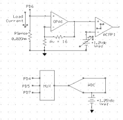
Disconnect due to overcurrent occurs within a couple of microseconds (ACMP interrupt latency) of that event. If the current across RSENSE is measured to be more than about 6 A, this will trip the ACMP regardless of pass element temperature (Fig. 6). Within the ACMP interrupt service routine (ISR), GPIO PB11 gets pulled low, which will turn off Q4, Q3.
This type of disconnect also puts the code into the fault condition—after every ~7.8 seconds, if the thermal considerations permit, this will disable PB11 as a GPIO and transit into a new analog voltage ramp to the gate of Q3. If that results in another short-circuit trip, then a new retry will occur after another 7.8 seconds if thermal considerations allow, and so on.
Figure 7 shows the flow of code execution involving the entire load switching action. The system level, code execution flow diagram shows how the thermal algorithm fits in.
A final consideration regarding load switching is that, whenever the short occurs, it connects VBATT across the buzzer, therefore providing an audio signal of the event. The sections above cover the load switching of the smart fuse.
Bang-Bang Switcher
Now, let’s take a closer look at the negative-to-positive bang-bang switcher’s unique characteristics. It’s bang-bang because the control loop is discontinuous; i.e., it’s controlled by ACMP with fixed thresholds and includes hysteresis to prevent unwanted oscillations.
The important considerations for this switcher include:
- It must switch at a relatively high frequency (low TON) to keep the size of the inductor reasonably small.
- The magnitude of the inductance should be high enough to keep the peak inductor currents low enough to correspond with the small physical size.
- The inductor ESR is low enough that I2 * R losses are ignored.
- It must accommodate an input voltage range from ~ 12 V dc to 14.5 V dc (with and without alternator charging).
- The overall energy transfer per inductor charge cycle to C1 (20 µF) should result in millivolt overall voltage increments to AVDD when taking into account Schottky D1 + series diode clamp losses, and the current flowing into the microcontroller to power the switcher while on, and for the rest of the system when the switcher is off. This is because AVDD sinks to 3.4 and is then charged to 3.426. For example, you can’t have so much energy transferred per charge cycle whereby AVDD exceeds the upper threshold in a single transfer.
- The inductor must fully discharge (discontinuous mode operation: have a long enough t-off) on each charge cycle to avoid building up the inductor current so much that it might either saturate, or overvoltage, AVDD at > 3.8 V dc.
- Nothing may be allowed to interrupt the inductor charge period, which otherwise would significantly increase the inductor energy or possibly even saturate the inductor. As a result, TIMER0, which determines the charge/discharge periods, must be given the highest interrupt priority in the system. The AVDDVMON that works together with TIMER0 is given the next highest priority to turn TIMER0 on/off also without interruption. This avoids overshoot/undershoot of the power supply voltage.
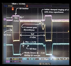
- Q2’s gate is quickly charged by Q5 to turn it on, but relies on passive turn-off through gate charge dissipation via R7. This adds ~1 µs to the inductor charge time on each cycle and must be taken into consideration.
- When the switcher is off, L1 forms a short between R11 and GND to keep Q6 off. When L1 is charging, though, Q6 VBE is reverse-biased and nicely Zeners at ~ -7.5 V, which is acceptable because R11 limits the current.
Keep in mind that a standard Zener will not work, instead of the series diode/xistor clamp, here because of the following issues:
- The clamp voltage is too sloppy to clamp at 3.6 V on boot.
- The knee currents are too high during normal operation and would drag down AVDD between charge cycles.
The equations and constants used for the switcher are:
- VD (Schottky) average forward voltage = 0.35 V
- TON = 2.00 µs
- TOFF = 8.00 µs
- VIN = 12 V dc
- VOUT = 3.4 V dc
- L = 470 µH
- a = (VOUT + VD) * TOFF/L
- b = VIN * TON/L
- ILOAD ~= 3 mA, average
- Inductor energy per charge cycle ~= b^2 * (L/2) = A
- Loss in Schottky ~= b * VD * TOFF / (√(3) = B
- Loss in series diode clamp (knee current) = VOUT * IKNEE * (TON) = C
- IKNEE is a function of temperature and is on the order of mA.
- Energy into C1 per charge cycle after Schottky and series diode clamp losses ~= A − B − C
- Energy out of C1 due to current flowing into MCU ~= VOUT * ILOAD * (TON + TOFF) = D (on the order of mA)
- Net energy into C1 during charge cycle ~= A − B − C − D
- Increase in C1 voltage after first charge cycle = √((A − B − C − D ) * 2 / (2 * 10−5) + VOUT2)
A spreadsheet can be used to determine the increase in C1 voltage per charge cycle thereafter. The very last term in the final equation above (VOUT2) is changed so that it assumes the previously increased value from the preceding charge cycle, until the 3.426 V dc threshold is reached or exceeded. My calculations resulted in the following AVDD voltages after each inductor charge increment:
Each charge cycle pushed the AVDD voltage higher by ~3.5 to 4 mV
Switcher performance is further highlighted visually (Fig. 8). Note that the inductor current goes discontinuous about 1 µs before the onset of the next charge cycle. This allows the inductor current to remain discontinuous as VBATT increases to ~14.5 V during alternator charging.
Going beyond those detailed power-supply considerations, all of the required functional blocks for a complete data-acquisition system are present in the Tiny Gecko microcontroller. Another channel is added to the ADC to measure OPA1’s output voltage (gained load current) whenever taking the thermistor readings.
The bang-bang power-supply considerations are important because time is needed between the charging bursts for temperature measurements. Time also is needed for ADC reconfiguration, load current measurement, data storage for subsequent retrieval, and then re-initialization of the ADC for the next round of measurements half a second later.
Data Storage
One way to store the measured thermal and load current data is in non-volatile flash using a Silicon Labs proprietary, wear-leveling library called NVM3. The data can be structured as 32-bit words containing 4 bytes as follows:
- Bits 31-24: load current
- Bits 23-16: T1
- Bits 15-8: T2
- Bits 7-0: T3
where all 12-bit ADC conversion are right-shifted by 4 bits for data storage. The loss of the 4 least significant bits (LSB) represent errors less than or equal to 1% in all temperature cases and for load currents over 300 mA.
NVM3 storage of a single 32-bit word to flash takes about 82 µs, so about 200 µs between bang-bang bursts is more than adequate. The word-write is a blocking function and must occur when the power supply isn’t switching to avoid overcharging the inductor. This project includes an instance of NVM3; however, for expediency, we’ve taken a shortcut and stored the data in RAM. An end-user can easily modify the code to use the NVM3 instance.
Once the data is taken and after connecting to USART0 TX on J2, shorting JP1 will force the Tiny Gecko into upload mode and turn LED1 on hard. Once that’s on, removing JP1 will start data upload.
Data is uploaded as individual bytes, then shifted left 4 bits, and subsequently undergoes the following:
Let V = Data * 2.5/4095 (V)
- Load Current = V/16/0.02 (A)
RT = V * 10k / (3.426 – V)) (Ω)
- Tn = 1.053E-6 * RT2 – 0.0181 * RT + 107 (25°C <= Centigrade <= 100 C)
Figure 9 shows 51 performance points over nearly a half-hour period. I’ve taken full data each half second (3,060 stored 32-bit words), but uploading for only each half-minute. For upload, PB7 is repurposed as USART0 TX. No RX is shown in the schematic, but the code is ready to be enabled on PB8 if desired.
The graphs show the data-acquisition system storing half-second current and temperature data. Over the 25.5-minute measurement interval, the load current was mostly between 30 and 60 mA and occasionally sank to below 30 mA. The measurement system can actually resolve 1.9 mA, but the chart shows increments of 30 mA because of the shift truncation of the ADC measurements to store the data as bytes. Against full scale 6-A range, 30 mA is only ~ one-half of 1%, so the truncation is acceptable in this case.
The temperature data shows a gentle rise over the nearly half-hour period but no significant Q1, Q3 temperature rise as the load current remained very low during the test. The difference in T1 vs. T2, T3 is likely due to its location on the breadboard and orientation inside of the cardboard box during the test.
I opened the lid to check on the LED during points 15-23 and the air conditioning affected the reading. The slightly higher reading after that is likely due to Q1 drain being directly connected to L1, which is constantly switching and has small I2*R heat buildup with no board metal to dissipate it.
Further testing should reveal more about the nature of the loads on this fused circuit. Overall, this project has been a BLAST to develop, and I encourage the automobile industry to implement this test functionality to better understand the interaction of common-fused loads. It may enable a reduction in overall wire thickness and thus vehicle weight for improved mileage, and cost.
Other important considerations:
- The smart fuse must include extra safety precautions in case the MCU quits operating for some reason. From bootup, a watchdog timer is operating with an ISR serviced every ~100 ms to clear it. If the WDT isn’t cleared, it will issue a system reset after ~ 120 ms. Only a power-cycle event at SW1 can restart the smart fuse in this event.
- As a final level of absolute protection, F1, a fast-blow 8-A fuse, is included. If all else fails, this fuse will blow to protect everything, so you can live to fuse another day.
- The smart fuse is scalable when using larger Q1, Q3 pass transistors such that analyses can be done on fused loads of even ≥ 30 A.
- This smart fuse is designed so that the Debugger/Programmer can power the system through the 10-pin Cortex connector (J1)—even when VBATT isn’t present—for development, troubleshooting, and/or data retrieval. When operating in debug mode, the AVDDVMON threshold can be changed in the code from 3400 to 2900, which will prevent the bang-bang from operating while everything else works.
- The following internal Tiny Gecko analog and digital peripherals are used in this project: TIMER0, AVDDVMON, OPA0, VDAC, OPA1, ACMP, ADC, CRYOTIMER, WDT, and USART0 (and NVM3). Code size is about 23.2 kB.
- The project may be downloaded for evaluation with Silicon Labs’ Simplicity Studio IDE

