BLDCs and Smart Gate-Drive Technology: A Match Made in (Power Tool) Heaven

Download this article in PDF format.
Cordless power tools are becoming the primary choice in both the professional and consumer markets for low-to-medium applications (Fig. 1). Workshop tools include screwdrivers, saws, drills, rotary hammers, and sanders. In the garden, there are clippers, grass trimmers, leaf blowers, and even chainsaws.

1. Cordless power tools and BLDC technology are beginning to dominate the market for low-to-medium power applications. (Source: Acme Tools)
In battery-powered tools, the search for longer battery life has led to the increasing adoption of brushless dc motors (BLDCs) to provide drive power. Compared to their brushed-motor counterparts, BLDCs have higher efficiency, higher torque-to-weight ratio, lower maintenance, higher reliability, and lower noise.
In the midst of all this goodness, there’s just one (tiny) fly in the ointment: Controlling a BLDC requires considerably more electronic circuitry than its less-efficient, noisier, short-lived, slower, and less-powerful predecessors.
A brushed dc motor has a wound armature (rotor) placed between the poles of a permanent or electromagnet (stator) and uses the brushes to mechanically switch current to the armature and cause it to rotate. In contrast, a BLDC has a wound stator and a permanent-magnet rotor assembly. The BLDC controller uses rotor position information from a sensor to electronically switch the stator windings in the correct sequence to maintain rotation of the magnet assembly.
Accomplishing this requires a more complex design. Figure 2 compares the drive circuits of a typical brushed and brushless motor. In contrast to the single gate driver and power FET of the brushed motor, the BLDC motor requires six FETs arranged into three half-bridge pairs, plus a gate driver for each FET. In a space-constrained application such as a power tool, this can tax the ingenuity of the packaging engineer, especially since power FETs have traditionally come in bulky packages such as TO-220, DPAK or D2PAK.
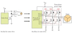
2. The BLDC demands a more complicated drive circuit than the earlier brushed DC motor. (Source: TI Motor Drive & Control Blog, Fig. 1)
The primary blocks in a BLDC controller are:
- A supervisory microcontroller unit (MCU), DSP, ASSP, or similar device to run the motor control algorithm
- A three-phase power stage with the required power capability
- A gate driver to drive the three-phase power stage
- A position sensor for accurate motor current commutation
- A power supply to power up the MCU and other blocks
What’s the best way to architect a BLDC controller design? Partition options run the gamut—it all depends on the application. You knew that, didn’t you?
A multi-chip design with each block separate allows each function to be optimized for the highest overall performance, but also has the highest part count, the highest cost, and longest design time.
At the other extreme, a single-chip BLDC controller or ASSP might be the answer for a high-volume, low-power application. This offers the quickest time-to-market, smallest size, lowest component count, and it has a feature set optimized for the target application. On the other hand, there’s likely to be very little flexibility or programmability.
A power tool requires a blend of these features. It doesn’t require the highest performance, but it does need programmability. Full-line tool suppliers have multiple products at a variety of power levels and price points, so including a low-power microcontroller gives designers the flexibility to change algorithms and scale power stages as needed.
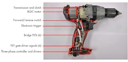
3. In a handheld power tool, there’s very little room for the electronic circuitry. In this example, the handle houses a complete BLDC controller. (Source: TI Motor Drive & Control Blog, Fig. 2)
When cramming all of these functions into the typical cordless tool (Fig. 3), it also means that the design must be very compact. Furthermore, it must be highly efficient so that it can maximize battery life. And did we mention low cost? That, too.
Power Tool Reference Design
Texas Instruments has developed an efficient, low-cost, BLDC reference design that’s suitable for power tools operating from a five-cell Li-ion battery pack with a supply voltage up to 21 V. The compact (65 × 60 mm) design can deliver up to 1 kW (50 A/20 V) and implements a trapezoidal control algorithm with sensor feedback.
Figure 4 shows the block diagram of the reference design. The main blocks are a control stage, based around the MSP430F5132 low-power MCU; a gate driver stage via the DRV8323 three-phase smart gate driver; and a power stage based around multiple CSD88584Q5DC Power Blocks. Other components include a TPS54061 synchronous buck converter to provide 3.3-V MCU power; an LMT87 precision temperature sensor; and a BLDC-mounted DRV5013 Hall-effect sensor for position feedback.
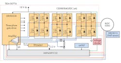
4. The TIDA-00774 reference design is a 1-kW three-phase BLDC controller optimized for power tools. (Source: TIDA-00774 PDF)
Let’s examine these stages in more detail.
Control Stage
The MSP430F5132 is a member of the MSP430 family of 16-bit reduced-instruction-set-computer (RISC) MCUs designed for portable applications. To maximize battery life, devices feature five low-power modes and can switch from low power to active operation in less than 5 μs.
MSP430 devices include different peripheral sets for various applications. The MSP430F5132 is a mixed-signal device. It incorporates a high-performance 10-bit, 200-ksample/s analog-to-digital converter (ADC), an on-chip comparator, a 32-bit hardware multiplier, two 16-bit high-resolution timers, two universal serial communication interfaces (USCIs), and up to 29 5-V-tolerant I/O pins.
The software affects PID control of the three-phase motor commutation via the PWM outputs of the MSP430. The PWM duty cycle controls the current through the power FETs and motor windings and, in turn, the speed of the motor.
If Hall sensors mounted on the motor are used, their signals reflect the motor position and are leveraged by the MSP430 to close the commutation loop. On capturing a Hall-sensor state-change event, the software updates the PWM outputs according to the commutation sequence.
An external potentiometer inputs 0 to VCC (3.3 V) to the MSP430 ADC and sets the motor speed. In the open-loop control implementation, this is the sole input to the control system. A closed-loop implementation also takes the actual motor speed via the Hall-sensor feedback.
Smart Gate-Driver Stage
The gate driver interfaces between the logic-level control outputs from the MCU and the half-bridge power stage. The gate driver must be able to accommodate a wide variety of external MOSFETs and external system conditions.
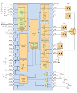
5. The DRV8232S includes multiple features to protect the power MOSFETs, reduce BOM count, and increase efficiency. (Source: DRV8320 datasheet)
Generally, a discrete gate driver offers designers more options, especially at high power levels. However, in this application, a smart gate driver is in many ways the key component because it integrates many of the control and power-stage functions into a single device. In this reference design, the DRV8323S smart driver (Fig. 5):
- drives the three-phase power stage with up to 1-A peak source current and 2-A peak sink current.
- incorporates multiple protection functions: undervoltage lockout, charge pump fault, MOSFET overcurrent, MOSFET short circuit, gate driver fault, and overtemperature.
- includes a serial peripheral interface (SPI) for fault reporting and changing of parameter values.
- implements a configurable trapezoidal PWM drive, freeing up MCU resources.
- measures the drain-source voltage (VDS) of the power FETs for accurate current sensing feedback.
The smart driver also contributes to maximizing overall efficiency—an important consideration in a battery-powered design—through more precise control of power FET operation during turn-on and turn-off.
The DRV8323S includes two proprietary features—IDRIVE and TDRIVE—that allow designers to adjust the VDS slew rate of the external power FET. The VDS slew rate is predominately determined by the rate of gate charge (or gate current) delivered during the FET QGD or Miller charging region, described in more detail here. By allowing the gate driver to adjust the gate current, it can effectively control the slew rate.
IDRIVE allows the DRV8323S to dynamically switch between gate drive currents via an SPI register setting. There are 16 IDRIVE settings ranging between 10-mA to 1-A source (IDRIVEP) and 20-mA to 2-A sink (IDRIVEN). The DRV8323S supplies the appropriate gate drive current for a selectable time tDRIVE to the gate during the turn-on or turn-off of the external power MOSFET. After the turn-on or turn-off period, the gate driver switches to a smaller current IHOLD to improve the gate driver efficiency.
Slew rate’s effect on switching efficiency is relatively well understood, but other effects are not as obvious.
Switch-node ringing is caused by the interaction between high slew rates and parasitic inductances and capacitances, both internal to the power FETs and external, due to PCB layout. This ringing can cause the switch-node voltage to drop below ground or rise above the supply, exceeding the specification limits of the gate driver or power FET, and resulting in catastrophic breakdowns.
Controlling the VDS slew rate is also a critical factor for optimizing radiated emissions, the energy and the duration of diode-recovery spikes, dV/dt gate turn-on leading to shoot-through, and switching voltage transients related to parasitics in the external half-bridge.
In addition to the IDRIVE slew-rate control, the DRV8323S also includes TDRIVE: an internal gate-drive state machine that optimizes the dead time between high-side and low-side switching, protects against inadvertent dV/dt gate turn-on, and monitors for excessive current to the MOSFET gate.
These two features result in a robust, protected, and efficient motor-drive system with minimal external overhead. You can find out more about power FET behavior and the IDRIVE and TDRIVE features in this Application Report.
Power Stage
The power stage is the final block in the power-tool reference design. The design uses two CSD88584Q5DC 40-V Power Blocks in parallel for each phase (six total) to deliver 50-A RMS continuous (120 A peak for three seconds, 160 A peak for one second) winding current.
The CSD88584Q5DC 40-V Power Block uses two NexFET devices packaged in a stacked-die technology to minimize parasitic inductances—especially common-source inductance (LCSI)—while offering a complete half-bridge in a space-saving thermally enhanced DualCool 5-× 6-mm package. NexFET is Texas Instruments’ third-generation macrocell power MOSFET technology. It reduces parasitic capacitances by about fifty percent compared to second-generation TrenchFETs, while offering comparable RDS(ON).
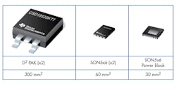
6. A three-dimensional stacked package can reduce the PCB footprint of a half-bridge driver by 50%. (Source: TI Motor Drive & Control Blog, Fig. 3)
With an exposed metal top, the DualCool package allows for the design of simple heat-sink applications that extract heat through the top of the package and away from the PCB. This provides superior thermal performance at the higher currents demanded by BLDC applications. Figure 6 compares the space needed for a half-bridge using two traditional power packages versus using a Power Block package.
When connecting power FETs in parallel, current sharing becomes very important. Ideally, each FET should carry equal current so that the losses are equally distributed.
The FET operation can be split into the conduction phase and the switching phase. In the conduction phase, both FETs are in the ON state, and the main parameter influencing current sharing is the RDS(ON) of each device. If the RDS(ON) values of the FETs aren’t equal, then the FET with the lowest RDS(ON) carries the highest current. This FET then has the most conduction losses, causing a rise in its temperature. Since MOSFETs have a positive temperature coefficient of on-resistance, higher temperature causes the RDS(ON) of the FET to increase, which in turn reduces the current. This self-regulating mechanism acts to gradually equalize the current through each FET.
The current-sharing behavior during the switching phase of the FET is a more complex phenomenon. It’s affected by asymmetries in the gate-drive circuit, differences in circuit parasitics, and variations in FET parameters such as transconductance (gFS), threshold voltage (VTH), and the input capacitances (CGD and CGS). A detailed discussion is beyond the scope of this article, but the topic is covered in depth in the Reference Design Guide.
About the Author
Paul Pickering
Paul Pickering has over 35 years of engineering and marketing experience, including stints in automotive electronics, precision analog, power semiconductors, flight simulation and robotics. Originally from the North-East of England, he has lived and worked in Europe, the US, and Japan. He has a B.Sc. (Hons) in Physics & Electronics from Royal Holloway College, University of London, and has done graduate work at Tulsa University. In his spare time, he plays and teaches the guitar in the Phoenix, Ariz. area
Comment About the Article
To join the conversation, and become an exclusive member of Electronic Design, create an account today!

Leaders relevant to this article: