A Clever Voltage-Fed Half-Bridge Converter Architecture
Download this article in PDF format.
Design engineers often turn to push-pull, half-bridge, and full-bridge power-converter designs for higher power output. These architectures show up from 200 W to 500 W and beyond. When space or weight is a constraint, it may also make sense to use a cascaded converter, where a buck regulator applies a voltage to those architectures to do the regulation. This means you set up the power transformer to use a 50% duty cycle—it’s a simple dc-dc transformer with no pulse width modulation (PWM).
Because the transformer is working at 50% duty cycle, you can minimize its weight and size. The wide duty cycle might allow you to use switching frequencies and magnetic materials that will also reduce weight, size, and cost. In terms of reducing transformer size, the push-pull architecture does not make as much sense. It lacks the winding efficiency, sometimes called copper efficiency, of the half- and full-bridge designs. With a push-pull design, you are only using half of the primary winding at any given time. Two coils are used to reverse the magnetic flux in the core, as opposed to reversing the current in a single coil by reversing the applied voltage.
Half-Bridge vs. Full-Bridge
There are tradeoffs between using a half- or full-bridge design. A half-bridge is likely to have a higher calculated reliability, since a capacitor will have a better rating than an active device. It will also have a simpler control scheme, since you only need to drive two transistors. The two capacitors will be cheaper than the added two transistors in a full bridge design. For military-specification (mil-spec) designs, the cost difference can be significant.
You can set up a full-bridge to be current-fed. This means that the buck pre-regulator does not have an output capacitor. This means you need to ensure there’s no dead time in the bridge excitation cycles. Indeed, you must ensure overlap, so that the current from the buck regulator has someplace to go at all times in the switching cycle.
The overlap in the current-fed full-bridge driving waveforms allow you to remove any filter inductors from the outputs of the converter. This means there will be very good cross-regulation in multi-output designs. It also gives the outputs very good transient response, since the lack of output inductors means that all capacitors on all outputs will help offset a transient event on any one output.
For lower-power outputs, you might get away with no output inductors on a half-bridge design. You have to examine the ripple currents you will get in the output capacitors, and the subsequent ripple voltage that appears in the regulated voltage. Because one leg in a half-bridge is formed by two capacitors, it’s always a voltage-fed design. The capacitors that form the half-bridge will also be output capacitors for the buck pre-regulator (Fig. 1).
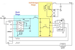
1. You can feed a half-bridge converter with a buck regulator to make a voltage-fed half-bridge converter. (Courtesy of Bob Bell and Texas Instruments)
Half-Bridge Advantages
One advantage of the half-bridge is that the primary-side transistors are only exposed to half the voltage compared to a push-pull design. This means you can use cheaper transistors with lower on-resistance. The capacitors that form one leg of the bridge means there’s no dc current that could ratchet up the flux in the core until it saturates. The capacitors also mean there’s only so much energy available that the FETs have to withstand. This can make the half-bridge more robust than a full-bridge.
A Real-World Example
I was exposed to the voltage-fed half-bridge cascaded converter when I worked on a power supply for the radar jamming pod in an F-16 fighter plane (Fig. 2). This was back in the 1990s, so not only was I constrained for part choices by the Qualified Parts List, (QPL), but the voltage and current ratings of the devices were not nearly as good as today.
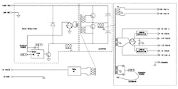
2. This voltage-fed half-bridge puts the buck regulator on the bottom to simplify the control and grounding scheme. The transformers are drawn to simplify the schematic, with dotted lines indicating a shared core.
One intriguing aspect of this design was that the buck regulator was on the low side of the cascade. This means that the buck-regulator control chip was referred to the common rail of the supply, and it could directly drive an N-channel FET. I can’t claim I invented this; I inherited the design, although it did not work properly. I saw no need to change the architecture. I just needed to size the components, add some features, and get the compensation of the loop perfected.
The design did not have to drop the incoming 265-V dc bus to start up. The startup was made easier by an external 15-V supply that came into the circuit board. It powered a simple oscillator that drove a transformer coil at 50% duty cycle. The secondary of that transformer, T1, would provide isolated drive to the gates of the half-bridge. It also had a startup coil that would power the control logic for the buck regulator. Once the supply came up, the startup power was overridden by power from the secondary of the main transformer, T2.
The startup power signal was also used to synchronize the buck section with the half-bridge. The running power from the main transformer T2 was used as the feedback to the buck-regulator chip. Since the outputs cross-regulate well, it was acceptable to just regulate the supply based on this sense coil output. The output of the supply was a two-phase, 90-V ac power rail, as well as ±15 V ac, ±15 V dc, and linear post regulators for a precise ±5 V dc.
The buck-regulator common is isolated from to the incoming 265-V dc common, while the output of the power supply has commons referenced to chassis ground, as indicated by the three schematic symbols. The “running power” secondary coil is referenced to the buck-regulator common. Note the freewheeling diode of the buck regulator is returning to the high-side power rail. This means the transistors on the switch node have to withstand the bus voltage.
The Schematic
I regret to say I did the schematics in PADS, but the 1993 version I used will not open in the free Mentor Graphics PADS viewer. I did find a DWG format drawing of the schematic (Fig. 3), but it’s not guaranteed to be correct since it’s not the PADS document that drove the board design. Because this was a mil-spec design, all of the components are hermetic. One very nice feature of the design is that both the buck and half-bridge sections use the same control chip, a UC1526A, the Unitrode chip now made by Texas Instruments. Not only did the control chip have to be in a hermetic ceramic DIP package, it also had to be available in mil-spec screening.
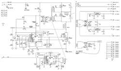
3. The detailed schematic reveals the design can use the same control chips and transistors for the buck and half-bridge sections. Note the thee distinctive ground symbols for input power, control power, and chassis common.
The feedback from the secondary feeds into a voltage divider formed by R5, R6, and R7, so technicians could tweak the output to give a precise output voltage. Since this design was for fighter jets owned by a foreign government, the hardware was not classified. However, the specifications were classified, so I don’t feel I can state the output currents and such, even if I could find those specs somewhere. You can infer the power from the two FETs on the buck regulator. The control IC drives two in parallel, so the power on each FET is halved.
As you would expect, the 2N6802 FET has a 500-V breakdown rating. This gives plenty of margin and improved reliability for switching the 265-V bus. The FETs have a 2.5-A rating, so that tells me the power of the supply could have easily been over 200 W. Just like using the same control ICs for the buck and half-bridge, the design also uses the same FETs.
There are 22-Ω resistors in the gate feeds of each transistor to prevent oscillations and add damping. This slows down the turn-on and turn-off, so it will increase switching losses. It will also reduce electromagnetic interference (EMI), although there are no FCC standards required for military electronics.
Small Size and Low Weight
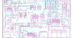
The design ended up fitting on a 3.3- by 3.6-in. circuit card (Fig. 4). Because this was flight hardware that had to go to 70,000 feet altitude, there was an aluminum heat frame under all of the components to take the heat toward clamps on the edge of the circuit board, then to the frame of the box, and then down to a liquid-cooled cold plate held at 65°C maximum. That makes the components rather spaced out, which led to a fight with the mechanical engineers who wanted the drawing for the heat frame to be simple, as opposed to having the components placed where they made the most electrical sense.
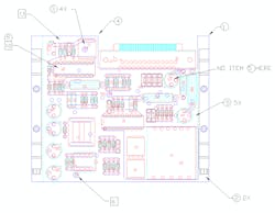
4. The voltage-fed half-bridge converter fits on a 3.3- by 3.5-in. circuit card assembly (CCA).
Doing mil-spec documentation is a great way to learn the right way to document your designs. This figure was part of the assembly drawing with all of the notations and revision control needed to build flight-ready hardware.
Military contractors were also pioneering the use of 3D design back in 1993 (Fig. 5). We used the 3D drawings I made in AutoCAD to ensure that all circuit boards went together properly. You can see the size of the main transformer to get an idea of the power this board could deliver. It looks to be a little over an inch square. The nice thing about half-bridge converters is that they get full utilization of the primary winding, unlike a push-pull that can only use half the primary at any given time. The push-pull also doubles the stress on the bridge transistors. A push-pull is like a teeter-totter. When one transistor pulls its primary leg down, the other primary leg swings just as high above the power rail.
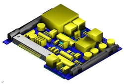
5. A 3D view of the voltage-fed half-bridge converter helps integrate it into the mechanical design, as well as allowing you to see the compact size and low weight needed in an F-16 fighter jet. The blue component is an aluminum heat frame that carries heat to the gray side clamps on the board assembly.
You could improve a modern design with much smaller surface-mount components. The TO-39 metal-can transistors could be in a ceramic SOIC. If you don’t need hermaticity, then you have even more choices. The clever “upside-down” architecture might not be as clever these days, since there are so many gate-driver chips and isolation chips available (Fig. 1, again). Still, if those new parts are not available mil-spec, then this clever design might get you out of a bind.

About the Author

Paul Rako
Creative Director
Paul Rako is a creative director for Rako Studios. After attending GMI (now Kettering University) and the University of Michigan, he worked as an auto engineer in Detroit. He moved to Silicon Valley to start an engineering consulting company. After his share of startups and contract work, he became an apps engineer at National Semiconductor and a marketing maven at Analog Devices and Atmel. He also had a five-year stint at EDN magazine on the analog beat. His interests include politics, philosophy, motorcycles, and making music and videos. He has six Harley Sportsters, a studio full of musical instruments, a complete laboratory, and a video set at Tranquility Base, his home office in Sun City Center Florida.
Comment About the Article
To join the conversation, and become an exclusive member of Electronic Design, create an account today!

Leaders relevant to this article: