FPGA Kit Detects USB Type-C Configuration Channel Signals
This file type includes high-resolution graphics and schematics when applicable.
Adoption of USB Type-C connector technology, along with the new USB Power Delivery (USB PD) specification, has been significant and swift. Many leading companies now support the new technology, and it’s already available on existing microcontrollers or with FPGAs for early adopters.
USB PD uses USB Type-C port's Configuration Channel (CC) signal line as a medium of transport for its power negotiations and alternate modes. The USB PD physical layer uses biphase mark coding (BMC) to transfer data over this CC signal line. The challenge is to decode the USB PD BMC data in a FPGA setup.
The USB Power Delivery (USB PD) physical layer employs the BMC scheme in its physical layer to transmit USB PD messages, with dc-coupled baseband signaling on the CC line to transmit data (ref. 1, chapter 5). In BMC coding (Fig. 1), there’s a transition every bit-unit time and a second transition in the middle when a 1 is transmitted.
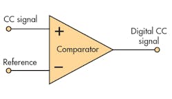
The voltage swing of this BMC signals on the CC line is defined as “vSwing” in the range of ≈0 V to ≈1.1 V by the USB PD specification. The specification also defines the center or midpoint voltage of the pulse as close to half of “vSwing.” Thus, a comparator and a reference voltage that indicates the midpoint is required to convert this BMC signal from the analog domain to the digital domain (Fig. 2).
The circuit converts a given BMC signal over the CC signal line to a 0 or 1 that’s readable by “soft logics,” which can then collate these bits to form the actual USB PD packet received. Most of the FPGA families have low-voltage differential-signaling (LVDS) I/O as an option in their configurable I/O options.
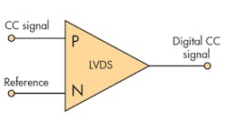
Therefore, the comparator required for USB PD BMC signaling can be created on a FPGA’s LVDS I/O by feeding a fixed reference voltage (Fig. 3). Since CC data signals swing between 0 and 1.1 V, and for easier understanding and setup, a mid-point closer to ≈0.55 V will be used as a reference input for one of the LVDS pins.
Step 1: Xilinx Zynq design of USB Type-C/USB PD BMC signaling
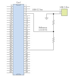
An FPGA-based system would be well-suited to explore using LVDS I/O to implement decoding of BMC signaling. The Xilinx Zynq combines programming logic and programming systems to implement and verify new technologies such as the USB Type-C/USB PD; here, we’ll use the Avnet MicroZed board based on the Xilinx Zynq platform. The circuit in Figure 4, based on the MicroZed Breakout Carrier Card Hardware User Guide2 uses Zynq’s Bank 34 T10/T11 differential pair to demonstrate BMC signal decoding.
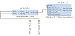
Using the Xilinx Vivado design suite,3 the reference voltage and the BMC signal are mapped as differential signals using the “util_ds_buf” library (Fig. 5). The Utility Differential Signaling Buffer generates buffers to bring off-chip differential signals into the USB Type-C IP for packetizing and processing the BMC data.
Step 2: Setting up LVDS I/O pins
After creating the design, the next step is to set up the constraints and map differential pairs pins connected to utils_ds_buf to the appropriate Zynq pins, here with differential pair LVDS_0_P (T11/T10) of Bank 34 selected (Fig. 6).
Having successfully set up necessary constraints and design in Vivado, the next step is to generate the bit stream and program on the board to see the BMC signals in digital domain. Additional debug mechanisms can be added to monitor the signal received in methods detailed by Vivado guides.
While the CC signal can be received in a system with simple capabilities such as a comparator, there are additional functions, including connect/disconnect detection, transmit logic, and BMC eye-diagram quality, that should be implemented for a fully functional USB Type-C/USB PD system.
Rajaram Regupathy holds a master’s degree in software systems from the Birla Institute of Technology & Science (BITS) in Pilani, India, and has 15 years of professional experience in developing firmware and system software embedded products. He has worked on USB technology from USB 1.1 to USB Type-C for leading semiconductor companies like Oki Semiconductor, NXP, ST-Ericsson, and Cypress Semiconductor, and has written three books about USB technology. He also has experience with other connectivity technologies like smart-card protocols (ISO7816, EMV), Bluetooth, and language processing tools.
References:
1. USB Power Delivery Specification, Revision 3.1
2. MicroZed Breakout Carrier Card User's Guide.
4. USB C-Thru
Looking for parts? Go to SourceESB.
