Improved Power-Factor Corrector Further Minimizes Miller Effect
>> Electronic Design Resources
.. >> Library: Article Series
.. .. >> Series: Ideas for Design
.. .. .. >> Ideas for Design Vol. 1
Download this article as a PDF file
In “Cascode Configuration Removes Miller Effect, Boosts PFC Performance," a cascode connection of two MOSFETs helped eliminate the Miller effect and significantly improve power factor correction (PFC) performance.
Recall that the Miller effect is a very large increase in a transistor’s apparent input capacitance due to negative feedback from the transistor’s output to input, when the transistor comprises a high-gain amplifier. A unity-gain amplifier has no Miller effect, although it may have a huge input capacitance and cause subsequent effects such as leading-edge and trailing-edge distortion associated with this input capacitance, and a charge-versus-voltage characteristic plateau.
However, the schematic that was tested and published was less than perfect for an important reason: the upper-cascode MOSFET input capacitance, Cgs, did not have a reliable discharge path. The improved design described here removes that downside and presents a viable cascode PFC schematic layout. Values and models of components used are just for demonstration and may differ depending on the purpose of the design.
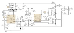
The cascode PFC design is built around MOSFETs M1, M2, and M3 (Fig. 1). The previous schematic does not have M3, which serves as the M2 Cgs discharge switch. This MOSFET significantly improves the PFC characteristics, expanding the upper operating frequency if driven properly.
P-channel MOSFET M3 should be controlled in-phase with the M1. An inexpensive low-voltage moderate RDS(on) transistor can be used here. Voltage source V3 represents a 12-V dc gate offset for M2, and it should be bypassed with a 10-μF ceramic capacitor. Both M1 and M3 work best if driven from a two-channel MOSFET driver such as the LTC1693-1 (Linear Technology Corp.) or similar.
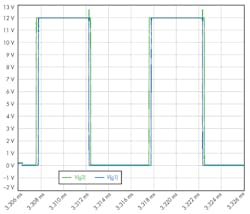
It is important to create proper gate-drive signals for M1 and M3 (Fig. 2). Transistor M3 should turn off earlier and turn on later than M1 to prevent a shoot-through current from the voltage source V3 through closed M3 and M1.
Two delay lines, whose parameters depend on the MOSFETs used, create the control voltage for M1 and M3. These delay lines are built on similar low-pass filters comprising resistors R5 and R6, capacitors C1 and C2, and diode D2 as well as symmetric counterparts R8, R9, C5, C6, and D1. A MOSFET driver with Schmitt triggers at the inputs is best.
Integrated circuit U2 is an example of an available PFC chip. The supply line is replaced with power source V1, and diodes D4 through D7 form a line rectifier. Almost any adequate power diodes can be used here.
IC U2 creates a pulse-width modulated control signal across resistor R17, which splits into two delay lines. When passed through the delay lines, it undergoes different delays of the leading and trailing edges due to the delay lines in both channels. This is how the gate-drive voltages of MOSFETs M1 and M3 are generated (Fig. 2, again).
About the Author
Gregory Mirsky
Princpal Electrical Engineer
Gregory Mirsky is a principal electrical engineer at Atlas Materials Testing Company (an Ametek Company). He holds an MS from the St. Petersburg Baltic Technical University, Russia, and a PhD from the Moscow State Pedagogical University.
Voice Your Opinion!
To join the conversation, and become an exclusive member of Electronic Design, create an account today!

Leaders relevant to this article:


