The analog and digital worlds have joined forces in Microchip’s Digitally Enhanced Power Analog (DEPA) hybrid controllers. These power-supply controllers contain analog control loops with digital oversight using analog references, amplifiers, and pulse-width modulation (PWM) to provide a regulated output. An embedded 8-bit PIC MCU configures, monitors, measures and dynamically adjusts power-supply performance. This allows the system to report telemetry, make operating adjustments on the fly, and respond to faults with customized, application-specific code stored in registers.
These single-chip solutions accept up to a 40-V input and regulate a wide output current or voltage range. Characteristics include tight regulation levels, fast transient responses, high gain, and phase margins required in server or telecommunications operation, all with the robustness and operating ranges required for automotive applications.
DEPA controllers provide advantages similar to PMBus:
- You can make performance modifications on an existing power supply using firmware changes rather than a soldering iron.
- A company can produce multiple power supplies with the same hardware while using unique firmware to customize each supply according to its application.
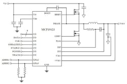
One of the new DEPA products is the 24-pin, 4- × 4-mm QFN, MCP19122/3 that applies traditional analog control circuitry to regulate the output of a synchronous buck dc-dc converter (Fig. 1). It has an integrated PIC microcontroller mid-range core, high-endurance flash memory, and communication and configurable analog circuitry. Integration with the PIC microcontroller provides complete customization of device operating parameters, startup and shutdown profiles, protection levels, and fault-handling procedures. These devices are able to efficiently convert 4.5- to 40-V inputs to 0.3- to 16-V outputs. The device’s characteristics are provided below.
1. The MCP19123 drives two external power MOSFETs for a programmable 0.3- to 16-V output with 0.1% typical accuracy.
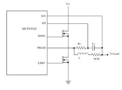
The system output current can be sensed by using either a low-value resistor placed in series with the output or for applications that require the highest possible efficiency of the inductor’s series resistance (DCR). For applications that use DCR sensing, a resistor in series with a capacitor are placed around the inductor (Fig. 2).
2. Inductor current-sense filter.
Synchronous buck features
- Switching frequency: 100 kHz to 1.6 MHz
- Multiphase systems
- Multiple-output systems
- AEC-Q100 qualified
- Configurable parameters
- Thermal shutdown
Microcontroller features
- Interrupt-capable
- Only 35 instructions to learn
- 4096-word on-chip program memory
- High-endurance flash memory
- Programmable code protection
- In-circuit debug (ICD) via two pins (MCP19123)
- In-circuit serial programming (ICSP) via two pins
- 12 I/O pins and one-input-only pin (MCP19122)
- 16 I/O Pins and one-input-only pin (MCP19123)
- 10-bit (ADC)
- On-chip timers
- I2C communication
CPU
CPU features in the MCP19122/3 include:
- Power-on reset (POR)
- Power-up timer (PWRT)
- Brown-out reset (BOR)
- Interrupts
- Watchdog timer (WDT)
- Oscillator selection
- Sleep
- Code protection
- ID locations
- In-circuit serial programming
Analog-To-Digital Converter (ADC)
An on-chip ADC accepts analog inputs that are multiplexed into a single sample-and-hold circuit. The output of the sample-and-hold connects to the input of the converter. The converter generates a 10-bit binary result via successive approximation and stores the conversion result into the ADC result registers.
I/O Ports
In general, when a peripheral is enabled, that pin may not be used as a general-purpose I/O pin. Each port has two registers for its operation:
- TRISGPx registers (data direction register)
- PORTGPx registers (reads the levels on the pins of the device)
Some ports may have one or more of the following additional registers:
- ANSELx (analog select)
- WPUx (weak pull-up)
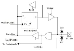
Ports with analog functions also have an ANSELx register, which can disable the digital input and save power. A simplified model of a generic I/O port, without the interfaces to other peripherals, is shown in Figure 3.
3. Shown is a simplified model of a generic I/O port, without other peripheral interfaces.
PMBus commands can be supported by the I2C interface if appropriate firmware is written into the device; there’s no native PMBus support in hardware. Microchip provides a reference firmware example supporting PMBus commands as part of its support environment, a GUI, and user guide that’s available on the company’s website.
Power-Supply Operational Parameter Registers
Data is stored in registers by using a write command to the correct address in memory. The memory map in the datasheet contains the file addresses for the calibration words and status registers.
Input overvoltage lockout: The VINOVLO register contains the digital value that sets the input over voltage lockout.
Input under/overvoltage control register: The VINCON register is the comparator control register for both the input undervoltage lockout and input overvoltage lockout.
Output overcurrent: A register stores the cycle- by-cycle peak current limit.
Current-sense gain: The entire current sense path has a fixed gain of 32. Additional gain or attenuation can be added using the CSGSCON register.
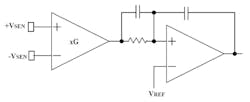
Compensation setting: The CMPZCON register is used to adjust the compensation zero frequency and gain (Fig. 4).
4. Simplified compensation.
Slope compensation ramp: A register stores data for adding slope compensation ramp to the current-sense signal, preventing this oscillation.
Reference-voltage configuration: Configuration of the 10-bit reference DAC is accomplished by the settings contained in the VOUTH and VOUTL registers. VOUTL is Output Voltage Set Point LSB and VOUTH is Output Voltage Set Point MSB.
Differential-amplifier gain control: The MCP19122/3 contains a low-offset programmable-gain differential amplifier used for remote sensing of the output voltage. The programmable-gain settings are controlled by the DAGCON register.
Output undervoltage: The output voltage is monitored and compared to an adjustable undervoltage (UV) reference. The output undervoltage reference is controlled by the VOTUVLO register.
Output voltage: The output voltage is monitored and compared to a stored overvoltage (OV) reference.
MOSFET driver dead time: Using the stored dead-time value, the MCP19122/3 can adjust both the high- and low-side driver dead time independently.
Analog peripheral control: The MCP19122/3 has various analog peripherals that can be configured to allow for customizable operation.
System configuration control: The MCP19122/3 can operate in a variety of different configurations. The MODECON register controls the system configuration of the MCP19122/3.
Overtemperature: The MCP19122/3 stores its hardware overtemperature shutdown protection, which is typically set at +160°C.
Device addressing: The communication address of the MCP19122/3 is stored in the SSPADD register. The MCP19122/3 contains a second address register, SSPADD2. This is a 7-bit address that can be used as the SMBus alert address when PMBus communication is used.
Device enable: A GPIO pin can be configured to be a device enable pin. By configuring the pin as an input, the PORT register or the interrupt on change (IOC) can be used to enable the device.
Relative efficiency measurement: The MCP19122/3 can measure the on-time of the high-side MOSFET. Therefore, the relative efficiency of the system can be measured and stored by changing the system parameters’ driver dead time, such as switching frequency.
Calibrate Word Registers
- Calibrate the overtemperature shutdown threshold point.
- Set the internal oscillator calibration.
- Calibrate the internal bandgap overtemperature.
- Calibrate the internal bandgap.
- Calibrate the internal 4.096-V bias voltage.
- Set the offset calibration for the output-voltage remote-sense differential amplifier.
- Calibrate the offset of the error amplifier.
- Calibrate the reference to the DAC that sets the output voltage reference.
- Calibrate the full-scale range of reference to the DAC, which sets the output-voltage reference.
- Calibrate the span of the slope compensation ramp.
- Calibrate the gain of the current-sense amplifier.
- Calibrate the output overvoltage and undervoltage comparators.
- Store the diode emulation-mode comparator offset voltage
- Store the calibration values for the offset voltage on the high-side current-sense amplifier.
- Store the ADC reading from the internal temperature sensor when the silicon temperature is at +25°C.
- Store the offset voltage of the unity gain buffer in units of millivolts.
- Store the calibration bits for the ADC.
- Store data to calibrate signals read by the A/D converter.
- Store the offset of the ADC.
- Set the calibration values to be used with different settings of the differential amplifier gain.
Instruction Set
The MCP19122/3 instruction set is highly orthogonal and comprises three basic categories:
- Byte-oriented operations
- Bit-oriented operations
- Literal and control operations
Each instruction is a 14-bit word divided into an opcode, which specifies the instruction type, and one or more operands, which further specify the operation of the instruction. There are 35 instructions.
In-Circuit Serial Programming (ICSP)
ICSP programming allows users to manufacture circuit boards with unprogrammed devices. Programming can be done after the assembly process, allowing the device to be programmed with the most recent firmware or a custom firmware.
Application Development
The MPLAB X Integrated Development Environment (IDE) is a software program that runs on a PC (Windows, Mac OS, Linux) to develop applications for Microchip microcontrollers and digital controllers. After initial device configuration using Microchip’s MPLAB X IDE software, PMBus commands or I2C can be used by a host to communicate with, or modify, the operation of the MCP19122/3.
MPLAB X IDE is flexible and friendly with complete project management, visual call graphs, a configurable watch window, and a feature-rich editor that includes code completion and context menus. With the ability to support multiple tools on multiple projects with simultaneous debugging, MPLAB X IDE is also suitable for the needs of new as well as experienced users.
About the Author

Sam Davis
Sam Davis was the editor-in-chief of Power Electronics Technology magazine and website that is now part of Electronic Design. He has 18 years experience in electronic engineering design and management, six years in public relations and 25 years as a trade press editor. He holds a BSEE from Case-Western Reserve University, and did graduate work at the same school and UCLA. Sam was the editor for PCIM, the predecessor to Power Electronics Technology, from 1984 to 2004. His engineering experience includes circuit and system design for Litton Systems, Bunker-Ramo, Rocketdyne, and Clevite Corporation.. Design tasks included analog circuits, display systems, power supplies, underwater ordnance systems, and test systems. He also served as a program manager for a Litton Systems Navy program.
Sam is the author of Computer Data Displays, a book published by Prentice-Hall in the U.S. and Japan in 1969. He is also a recipient of the Jesse Neal Award for trade press editorial excellence, and has one patent for naval ship construction that simplifies electronic system integration.
You can also check out his Power Electronics blog.


