Download this article in PDF format.
Printed-circuit-board (PCB) substrate material, like FR-4 glass epoxy, is a poor conductor of heat. Conversely, copper is an excellent conductor of heat. So, more copper area on a PCB is ideal from a thermal-management perspective.
Thick copper, like 2-oz. foil (68 microns thick), conducts heat better than thinner copper. Unfortunately, using thick copper is expensive, and makes it difficult to achieve fine geometries. Therefore, the use of 1-oz. (34 microns) copper has become commonplace. For external layers, this is often ½-oz. copper plated up to 1-oz. thickness.
Solid-copper planes used on inner layers of multi-layer boards work well to spread heat. However, since these planes are normally placed in the center of the board stack-up, the heat can get trapped inside the board. Adding copper areas on the outer layers of the PCB and placing many vias to connect, or “stitch,” these areas to the inner planes helps transfer heat out of the planes.
On two-layer PCBs, spreading heat may prove more difficult due to the presence of traces and components. Providing as much solid copper as possible with good thermal connections to the motor-driver IC is a necessity. Putting copper pours on both outer layers and stitching them together with many vias helps spread the heat across areas cut by traces and components.
Trace Width: Wider Is Better
Since the current in and out of a motor-driver IC is large (exceeding 10 A in some cases), carefully consider the width of PCB traces in and out of the device. The wider the trace, the lower the resistance. Traces must be sized so that excessive power isn’t dissipated in the trace resistance, which causes the trace to heat up. Too small of a trace can actually act like a fuse and burn open!
Designers often use the IPC-2221 standard to determine appropriate trace widths. This specification has charts that show the copper cross-sectional area for various current levels and allowable temperature rise, which can be converted to a trace width at a given copper-layer thickness. For example, a trace carrying 10 A of current in a 1-oz. copper layer needs to be just over 7 mm wide to achieve a temperature rise of 10°C. For a 1-A current, the width need only be 0.3 mm.
Given this fact, it seems impossible to run 10 A of current through a tiny IC pad.
It’s important to understand that the trace-width recommendations in IPC-2221 apply to a long PCB trace of constant width. It’s possible to pass much larger currents through a short section of PCB trace with no ill effects if they’re connected to a larger trace or copper area. This is because the resistance of the short, narrow PCB trace is small, and any heat generated there will be drawn into the wider copper areas, which act as a heat sink.
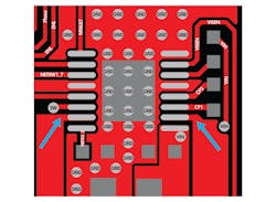
1. The PCB trace is widened so that the pads can better handle the continuous current.
For example, refer to Figure 1. Even though the pads for this device are only 0.4 mm wide, they must carry up to 3 A of continuous current. The trace is widened into as large a width as practical, and as close to the device as possible.
Any heat generated in the narrow portion of the trace is conducted to the wider copper areas so that the temperature rise in the narrow trace is negligible.
Traces embedded in the PCB on inner layers cannot dissipate heat as well as traces on the outer layers, because the insulating substrate doesn’t conduct heat well. For this reason, inner-layer traces should be designed to be about twice as wide as those on the outer layers.
As a rough guideline, the table shows recommended trace widths for long traces (more than ~2 cm) in motor-driver applications.
If space permits, routing using even wider traces or copper pours will minimize temperature rise and voltage drop.
Thermal Vias: Use As Many as Possible
Vias are small plated holes that are typically used to transport a signal trace from one layer to another. Thermal vias are made the same way, but instead transmit heat from one layer to another. The proper use of thermal vias is critical to heat dissipation on a PCB, but several manufacturability issues must be considered.
Vias have thermal resistance, which means that there’s some drop in temperature across them as heat flows through, measured in degrees Celsius per watt of power. To minimize this resistance and make the vias more effective at transmitting heat, the vias should be large with as much copper area inside the hole as possible (Fig. 2).
2. Vias (shown is a cross-section of a via) should be large and contain as much copper inside the hole as possible to minimize thermal resistance.
Although using large vias in open areas of the PCB is possible, vias are often placed within a pad area to move heat directly from the IC package. In this case, large vias aren’t possible. That’s because a large plated hole would cause “solder wicking,” where the solder intended to connect the IC to the PCB flows down into the via, leading to a poor solder joint.
There are several ways to reduce solder wicking. One is to use very small via holes so that the volume of solder wicked into the holes is small. However, small vias have more thermal resistance, so more are needed to achieve the same thermal performance.
Another technique used is to “tent” the vias on the backside of the board. This involves removing the opening in the solder mask on the backside so that the solder-mask material covers the via. If the via hole is small, the solder mask will plug the via; therefore, solder can’t wick through the PCB.
Unfortunately, this may also create a different problem: flux entrapment. With a plugged via, flux (which is a component of solder paste) could get trapped inside the via. Some flux formulations can be corrosive and result in reliability issues over time if they’re not removed. Luckily, most modern no-clean flux processes are non-corrosive and don’t cause problems.
Note that thermal vias should never have thermal reliefs. They must be connected directly to the copper areas (Fig. 3).
3. Thermal vias should directly connect to copper areas on the PCB.
It’s recommended that the PCB designer check with the surface-mount-technology (SMT) process engineers at the PCB assembler to choose the best via size and construction for that assembler’s process, especially when thermal vias are placed within pad areas.
Soldering Exposed Pads
TSSOP and QFN packages have a large exposed pad underneath the part. This pad, connected to the back side of the die, is used to remove heat from the device. It’s imperative that this pad be well-soldered to the PCB to dissipate power.
The opening in the stencil that’s used to deposit solder paste for this pad isn’t always specified on the IC datasheet. Often, SMT process engineers have their own rules about how much solder should be deposited and what sort of pattern should be used on the stencil.
If a single opening similar in size to the pad is used, a large amount of solder paste is deposited. This can cause the device to be lifted up due to the surface tension of the solder when it melts. Another concern is solder voiding (cavities or gaps inside areas of solder). Solder voiding occurs when the volatile component of flux vaporizes, or boils, during the solder reflow process. This can cause solder to be pushed out of the joint.
4. This solder stencil for a QFN package reveals four small openings to deposit paste on the central pad.
To address these issues, for pads that are more than about ~2 mm2, the paste is normally deposited in several small square or circular areas (Fig. 4). Dividing the paste into smaller areas allows the volatile flux components to more easily escape the paste without displacing the solder.
Again, it’s recommended that the PCB designer consult with SMT process engineers to design the correct stencil openings for these pads. A number of papers are available online that can help with this step, too.
Component Placement
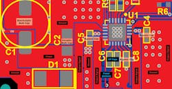
Component-placement guidelines for motor-driver ICs are similar to other types of power ICs. Bypass capacitors should be placed as close to the device power pins as possible with bulk capacitors located nearby. Many motor-driver ICs use bootstrap and/or charge-pump capacitors, which should also be placed near the IC.
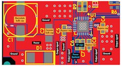
5. Here’s an example of good component placement on a two-layer PCB that includes an MP6600 stepper-motor driver.
Refer to Figure 5 for an example of good component placement. It shows an MP6600 stepper-motor driver on a two-layer PCB. Most signals are directly routed on the top layer. Power is routed from the bulk capacitors to the bypass and charge pump capacitors on the bottom layer, using multiple vias at the points where it changes layers.
In part two of this article, we’ll look at some specific motor-driver IC packages and how to implement PCB layouts using them.
About the Author
Pete Millett
Senior Technical Marketing Engineer
Pete Millett is a Senior Technical Marketing Engineer at Monolithic Power Systems (MPS). He has been defining and supporting motor-driver ICs for nearly 10 years. He previously worked as a board-level hardware design engineer in computer and consumer electronics industries for over 20 years.


