With Proper Isolation, You Won’t Need To Do The Safety Dance Around High Voltages
When we were children, my sister had a lamp with a yellow plastic base topped with a white globe in her bedroom—very cool, very 1960s. I loved turning it on and watching the globe glow. One day the plug had partially worked its way out of the wall, so I went to plug it back in. Unfortunately, my small fingers grabbed both of the prongs on the plug, and I received a nasty electric shock. I remember lying on the floor, looking at the ceiling, and wondering what happened. Getting shocked was no fun.
Protecting people from electrical hazards is serious business. There are numerous cases where people near hazardous voltages must be protected from them even in the event of a failure. Protection from these hazards can take many forms. For example, house wiring is covered with two dielectric insulating layers to protect the bare wire from being exposed.
Related Articles
• Drive Trains Face Unique Challenges In Electric Vehicles
• Industrial Energy-Efficiency Techniques Hit Residential Market
In many cases, systems need to communicate across a high-voltage barrier to send information or control signals between a low-voltage domain and a high-voltage domain. The voltages being isolated can peak at several thousand volts and run continuously at up to 1000 V. This communication requires the domains to be linked but isolated from each other. Isolation in the form of optocouplers, transformers, or modern CMOS capacitive-based isolation can be used to accomplish this task.
What Is Isolation?
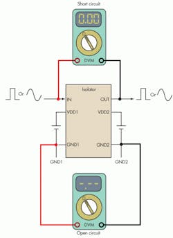
Isolation allows signals to be passed across a barrier while maintaining a very high impedance to minimize current flow across the barrier. An ideal isolator looks like a short to the signal being transmitted but is open to the current path for that signal (Fig. 1). Isolation can also be used to accomplish other tasks, such as level shifting a signal between a low-voltage microcontroller and a high-voltage power transistor driver or to remove ground noise in a precision measurement system (Fig. 2).
1. An ideal isolator offers an open current path for the signal while also appearing to be a short circuit.
2. Isolation tasks include safety isolation, level shifting, and eliminating ground noise.
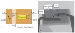
One of the oldest and most commonly used isolation devices is the optocoupler. Optocouplers work by using an LED to shine light onto a phototransistor. The phototransistor decodes the signal to reconstruct the signal at the device output. To have a reasonable voltage rating, most optocouplers use a dielectric film between the LED and output transistor (Fig. 3).
3. Optocouplers incorporate light emitting diodes, phototransistors, and an insulating dielectric film between these elements.
While optocouplers have served as primary isolating devices, they are plagued by a variety of issues including low operating speeds, poor channel densities, output current that varies over temperature and aging, poor device-to-device timing matching, and wear due to LED aging.
Modern Isolation Techniques
Modern semiconductor processes can be used to create extremely robust isolation barriers. While it may seem like a low-voltage CMOS cell-phone chip doesn’t experience much electric stress, the CMOS transistors used in billions of cell phones are subjected to extreme electric fields during their operation.
Consider a low-voltage MOSFET transistor in a fine geometry process. It may only have a voltage of 1.8 V across it, but the gate insulation that prevents a short between the gate and the rest of the transistor is extremely thin, on the order of 4 nm. This results in extremely high electric field strengths across the insulating material. Fields can be on the order 4.5 kV/µm, and the insulation must withstand these fields without an electrical failure over nearly continuous operation.
To prevent a breakdown, the insulating material, which is silicon dioxide (SiO2), must be extremely robust. By building a capacitor using SiO2 as the dielectric material, information can be sent across the capacitor, while safely insulating against high voltages without breakdowns (Fig. 4).
4. Modern CMOS isolation devices incorporate SiO2-based capacitors.
Using CMOS technology for isolation brings numerous advantages. CMOS is one of the most widely studied and used electrical materials. Foundries invest billions of dollars in fab process development and in characterizing the insulating properties of SiO2. All of this R&D can be put to use building isolators for very high voltages.
By developing isolators in CMOS, other functions can be easily and inexpensively added to the isolation. Features like embedded MCUs, analog-to-digital converters (ADCs), and threshold detectors can be integrated into the device. Multiple channels can be implemented on the same die, reducing the solution footprint and improving the channel-to-channel timing. Also, these channels can be run at extremely high speeds, up to 10 times faster than a typical optocoupler.
Using a semiconductor process to provide the insulation, rather than relying on dielectric tape inserted at packaging as used in an optocoupler, means that the insulation layer is well controlled and repeatably constructed. As mentioned earlier, the electrical insulating properties of SiO2 are outstanding compared to other dielectrics. It can withstand 10 times the electric field strength for the same thickness as the typical insulation tape used in an optocoupler.
Certifiably Safe
Depending on the application, isolation devices need to be certified by regulatory agencies before they can be used in a system. For example, a high-voltage motor controller may need regulatory certification to verify that the system and its components are safe. Several certification agencies, such as Underwriters Laboratories (UL) in North America and the VDE Institute in Europe, must be considered depending on the application and country.
Modern CMOS isolators are certified to numerous component industry standards such as IEC 60747-5. A version of this standard, IEC 60747-5-5, is intended exclusively for optocouplers, specifying minimum thickness for the insulating layers. An updated version, the IEC 60747-5-10 (currently in working stage), encompasses modern technologies such as digital isolators. This version accounts for differences in technology, such as the fact that modern isolators can operate with much thinner insulating layers to achieve the same level of performance as optocouplers. The new standard version stipulates the same rigorous test requirements and expected performance but removes the minimum insulation restriction.
Conclusion
As high-voltage electronics become more prevalent in our daily lives in systems such as electric drive trains, solar inverters, and motor controllers, the need to protect people who interact with these systems is crucial. Like all electronics, these systems are under pressure to reduce size, weight, and cost while allowing more features to be packed into an ever-shrinking space.
CMOS semiconductor isolators are bringing the same disruptive forces to bear on high-voltage isolation that are driving more advanced features and size reduction in smart phones and tablets. By incorporating modern CMOS isolation devices into these new high-voltage systems, manufacturers can ensure that their smaller, improved systems don’t give end users a nasty shock.
Ross Sabolcik is the director of Isolation products at Silicon Labs, providing strategic and product line marketing support for the company’s digital isolator, isolated gate driver, and current sensing products. He joined Silicon Labs in 1999 and has served as director for the company’s sub-GHz wireless products; director of applications and systems engineering for the company’s Broadcast products; director of applications engineering for Wireline products; and applications engineering manager for Isolation products. Prior to Silicon Labs, he worked at National Instruments, managing product development for embedded DSP and MCU firmware, as well as board-level hardware design for precision PC instrumentation. He holds a master’s degree in computer and systems engineering from Rensselaer Polytechnic Institute and a BSEE from Penn State University.
About the Author
Ross Sabolcik
Senior Vice President and General Manager for Industrial and Commercial IoT Products, Silicon Labs
Ross Sabolcik leads Silicon Labs’ Industrial and Commercial IoT business unit. He oversees the delivery of connected, wireless solutions for industrial and commercial sectors including metering, industrial and building automation, commercial lighting, and connected retail applications.
Ross joined Silicon Labs in 1999 and holds a Master’s degree in computer and systems engineering from Rensselaer Polytechnic Institute and a Bachelor’s degree in electrical engineering from Penn State University. He currently serves on the executive committee for Austin Habitat for Humanity.


