
Download this article in PDF format.
The world of power electronics witnessed a breakthrough in 1959 when Dawon Kahng and Martin Atalla invented the metal-oxide-semiconductor field-effect transistor (MOSFET) transistor at Bell Labs. The first commercial MOSFET was released to production five years later. Since then, generations of MOSFET transistors have enabled power designers to achieve performance and density levels not possible with their bipolar predecessors.
These advances, however, began to taper off in recent years, creating a vacuum and need for the next breakthrough technology. That’s where gallium nitride (GaN) comes into the picture.
A wide-bandgap transistor technology, GaN is creating an exciting opportunity to achieve new levels of performance and efficiency in power electronics systems. GaN’s inherent advantages open the doors for engineers to rethink power density in ways that weren’t possible before and meet the world’s increasing power demands. In this article, I’ll explore how.
Why GaN?
GaN offers several key benefits and advantages to silicon MOSFETs when it comes to power density, including:
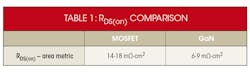
• Lower RDS(on): As shown in Table 1, GaN has half the RDS(on) per area of MOSFET. This directly translates to 50% lower conduction losses in the circuit. Thus, you can use smaller heat sinks and simpler thermal management in your designs.
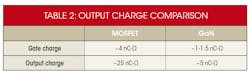
• Lower gate and output charge: GaN offers lower gate charge. A typical medium-voltage device has around 1 nC of gate charge compared with 4 nC for MOSFETs (Table 2). A lower gate charge enables designs with much faster turn-on times and slew rates, while reducing losses.
Similarly, GaN has a substantially lower output charge (Table 2, again), which brings a twofold advantage to each design. First, switching losses drop by as much as 80%, which in combination with lower conduction losses, has a major and positive impact on power density. Second, the design can run at much higher switching frequencies—up to 10X depending on the topology and application. This significantly reduces the size of magnetics as well as the size and footprint of designs, while improving overall efficiency by as much as 15%.
• Zero reverse recovery: Silicon MOSFETs have a typical reverse-recovery charge in the 50- to 60-nC range, depending on their size and characteristics. When the MOSFET turns off, the reverse-recovery charges (Qrr) in the body diode produce losses that add to the total system switching losses. These losses rise proportionally with switching frequency. As seen in Figure 1, the Qrr losses at higher frequencies make MOSFETs impractical in many applications.
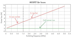
1. Reverse-recovery charge (Qrr) losses are much greater at higher frequencies with MOSFETs than GaN alternatives.
In contrast, GaN has zero reverse recovery and zero Qrr losses, making GaN FETs ideal for hard-switched applications, as will be shown in a later example.
Driving GaN
Regardless of the type of GaN used, gate-drive design is critical to achieving the best overall performance. A good analogy to a poor gate-drive design is using street tires on a Formula One racing car.
Keep several key parameters in mind when designing the gate driver, including:
• Bias voltage: It’s important to bias the gate with the optimal voltage to get the best switching performance, while protecting the gate against potential overvoltage conditions. Bias level varies by type and GaN fabrication process, and needs to be set accordingly. Having a clamping or overvoltage protection circuit is also very critical.
• Loop inductance: Because of GaN’s high slew rate and switching frequency, any parasitic inductance in the design introduces losses and ringing in the system. Many sources of inductance exist in a design, including leads and internal bond wires in both the GaN FET and driver packages, as well as printed-circuit-board (PCB) traces. Although you can reduce these, it’s very difficult to eliminate them. GaN power-stage solutions such as the LMG3410 integrate the driver and GaN FETs into a single package, significantly lowering overall inductance.
• Propagation delay: Short propagation delays and good matching (for half-bridge topologies) are very important for high-frequency operation. A propagation delay in the order of 25 ns and matching of 1 to 2 ns is a great starting point for high-frequency (1 MHz or higher) designs.
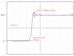
2. As evidenced with this GaN switching waveform of an optimized driver design, GaN can operate at very high slew rates, and there’s minimal ringing on the switch node.
With an optimal gate-drive design and PCB layout, you can operate GaN at very high slew rates (>100 V/ns) with minimal ringing on the switch node. Figure 2 shows an example of a switching waveform from such a design.
Design Example: Next-Gen PFC Solution
Due to its unique characteristics, GaN helps power designers overcome some of most difficult challenges of power density in different systems and applications. These gains don’t come from simply replacing a MOSFET with its GaN equivalent in an existing design. GaN enables new circuit topologies and/or operating modes that were previously not possible with silicon MOSFETs. The significant advantages lead to new classes of products with smaller size and improved efficiency. Let’s look at one such example.
Power factor correction (PFC) is mandatory in every electrical or electronic product consuming more than 75 W. PFC is the first power-conversion block that sits between the mains and the rest of the system, and carries the entire load at any given operating point. Thus, it directly impacts overall system size and efficiency.
Generations of different topologies have been designed with the goal of reducing size while meeting industry standards for efficiency. The efficiency levels defined in 80 Plus, for example, require 96% efficiency for titanium-grade power supplies.
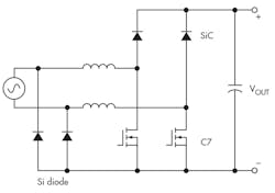
3. The dual-bridge PFC topology is often employed in many high-power designs.
Many high-power systems (>1 kW) use the dual-bridge topology (Fig. 3). We have seen density improvements in the last decade with the introduction of silicon-carbide (SiC) diodes and the latest generation of super-junction MOSFET transistors. These improvements, however, have reached a plateau in efficiency and power density.
A significant increase in power density requires an alternative approach that reduces:
• The number of power switches.
• The number of filter inductors.
• The size of the inductors.
• The size of heat sinks and cooling elements.
One alternative is the continuous-conduction-mode totem-pole topology. This topology takes advantage of all of GaN’s key characteristics, which ultimately leads to designs that are both smaller in size and higher in operating frequency (Fig. 4). GaN’s zero reverse recovery is particularly critical for implementing this topology.
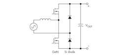
4. The totem-pole PFC topology, which reduces design size while boosting operating frequency, takes advantage of GaN’s zero reverse recovery.
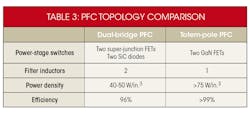
Table 3 summarizes several key benefits of this bridgeless PFC design. Expounding on them further:
• Power switches: In contrast with the dual-bridge topology, the totem-pole PFC replaces two super-junction MOSFETs and two SiC diodes with only two GaN devices.
• Filter inductors: This topology eliminates one bulky filter inductor in the power stage. The removal of the inductor, along with the reduced number of power switches, also improves overall system reliability.
• Size: Since GaN operates at a much higher switching frequency (typically four times compared to MOSFETs at 40 to 60 kHz), you can use a smaller filter inductor. In addition, GaN’s lower switching losses enable designers to significantly shrink the size of the heat sinks in the power stage.
• Efficiency: A well-designed totem-pole PFC operates at above 99% high-line efficiency. To put this in perspective, a 1-kW design dissipates less than 10 W in the entire PFC stage.
• Cost: GaN devices carry a higher premium because of their present manufacturing cost. However, given the savings outlined here, total system cost should be on par with existing MOSFET designs.
Modern totem-pole designs also leverage digital power controllers to further improve efficiency, total harmonic distortion, and other critical design parameters. Digital controllers, such as C2000 and UCD3138, can intelligently control the power-stage operation to optimize efficiency in real time, and in response to line and load conditions.
Conclusion
We’re witnessing an ever-increasing demand for higher power at much greater efficiencies in industries such as cloud computing, 5G telecom infrastructures, wind and solar farms, and electric and hybrid vehicles, to name just a few. With silicon MOSFETs reaching a plateau, designers are exploring wide-bandgap technologies such as GaN for their next design.
As shown in the PFC example, GaN not only improves efficiency, but dramatically reduces the size of the power supply by 30% to 50%. You can use GaN in isolated or non-isolated dc-dc converters, inverters, and other power-conversion subsystems to significantly reduce power losses, component counts, weight, and size.
Masoud Beheshti is responsible for advanced technology strategy and marketing for wide-bandgap solutions at Texas Instruments. Beheshti has years of experience in power management, serving in multiple roles that include system engineering, product-line management, and marketing and application management. He has a Bachelor’s in electrical engineering from Ryerson University and a Master of Business Administration in marketing and finance from Southern Methodist University.

About the Author
Comment About the Article
To join the conversation, and become an exclusive member of Electronic Design, create an account today!

Leaders relevant to this article: