Select The External Components For An Automotive SEPIC DC-DC Regulator
High-voltage SEPIC controllers have many automotive applications. They commonly are used as front-end regulators to regulate the main system voltage during a cold or warm crank when the battery voltage falls. They also are used during a load dump when the battery voltage rises.
This file type includes high resolution graphics and schematics when applicable.
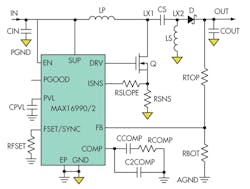
In fact, an automotive high-voltage SEPIC dc-dc power supply can be implemented using a 36-V, automotive boost SEPIC controller (Fig. 1). Designers can select the right external components to achieve the best system performance.
Component Selection
First, designers must define the basic parameters before they can select these components. Four principal design input parameters will influence the choice: switching frequency (fSW), output voltage (VOUT), output current range (IOUTMIN and IOUTMAX), and input voltage range (VINMIN and VINMAX).
The operating range of the controller used in the design will determine the switching frequency. The MAX16990, for example, has a switching frequency range of 100 kHz to 1 MHz, and the MAX16992 has a switching frequency range of 1 MHz to 2.5 MHz. Choose the controller and switching frequency best suited to your application. Using the principal design input parameters, we estimate the average input current range with:


where Eff is the estimated efficiency of the SEPIC regulator.
We assume an initial efficiency of 85% for 400-kHz operation and an efficiency of 80% for 2.2-MHz operation. Now specify all the external power components (nMOS, inductors, series capacitance, sense resistor, and rectifier diode), and then review and refine your design with a new useful calculator specifically created for the MAX16990 and MAX16992.
Next, we evaluate the duty-cycle range (DMIN and DMAX) in which the regulator operates. This can be determined with:
where:
VD is the forward voltage of the rectifier diode
RDS(ON) is the drain-source resistance of the nMOS when turned on
RSENSE is the sense resistor
You can ignore RSENSE in the equations for now. We will make a more accurate estimate of the duty-cycle range later. Nonetheless, ensure that the estimated duty-cycle range is within the specification of the selected device, in this case 4% to 93% for the MAX16990 and 24% to 85% for the MAX16992.
Inductors
Calculate the critical inductance for Lp and Ls with:


Choose a commercial value that is always higher than the critical inductance. This way, you guarantee continuous-conduction mode (CCM) operation throughout the application. Note that LpC and LsC halve their values if coupled inductors are used.
There is another parameter to remember when choosing proper inductors: the inductor current ripple ratio, or LIR. This parameter is defined as the ratio of the peak-to-peak inductor current and the average input current:

The relationship between the inductors (Lp and Ls) and the LIR is shown in:


LpLIR and LsLIR halve their values if coupled inductors are used.
To reduce losses, choose an inductor that guarantees an LIR between 0.3 and 0.5 (Figures 2 and 3).
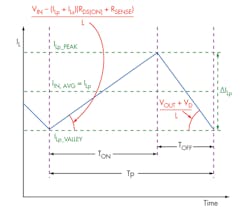
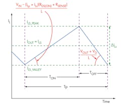
With L equal to LC, the LIR is 2. By increasing L further, you reduce the LIR. The selected inductors need to have a saturation current higher than their respective peak current, which is:


nMOS And Rectifier Diode
The peak nMOS drain current is the sum of the peak current of the two inductors:
InMOSPEAK = ILpPEAK + ILsPEAK (12)
The maximum drain-source voltage is equal to:
VnMOSDSMAX = VINMAX + VD + VOUT (13)
The average current that flows through the rectifier diode coincides with the output current, while the maximum reverse voltage is equal to:
VDREVMAX = VINMAX + VOUT (14)
Choose the rating of the two power components according to the above formulas.
Sense Resistor
Now that the peak nMOS current has been calculated, the sense resistor (RSENSE) can be selected. The MAX16990/MAX16992 trigger the current limit when the voltage on the ISNS pin reaches 212 mV (min). This voltage is due both to the drop on the sense resistor and to the drop on the slope resistor (RSLOPE), the latter of which is used for slope compensation. To leave 100 mV of room for slope compensation, it is initially recommended that RSENSE generate a voltage drop of 112 mV at the current-limit threshold. RSENSE is calculated with a current-limit threshold 20% higher than the peak inductor current:

Series Capacitor
The series capacitor is charged at a dc voltage equal to the input voltage. It must carry the primary inductor current during the off-time and the secondary inductor current during the on-time. This makes this capacitor selection challenging, even somewhat tricky.
As the first requirement, the voltage rating of the series capacitor has to be higher than the maximum input voltage (VINMAX). The RMS current flowing through the capacitor is given by:

The capacitor value and its equivalent series resistance (ESR) determine the ripple across the series capacitor. Assuming a 1% voltage ripple across the series capacitor due to the ESR, the series capacitor ESR has to be lower than:

Finally, the series capacitor value has to be high enough to guarantee a voltage ripple lower than 5%:

Output Capacitor
Selecting the correct output capacitor (COUT) and its related ESR is very important for minimizing output voltage ripple. Assume that the output voltage ripple (VOUT_RIPPLE) is equally distributed between the voltage drop, which is due to the capacitor discharging during off-time, and the ESR voltage drop. To find the minimum capacitance and the maximum ESR for the output capacitor, use:


Compensation
After reviewing these external components, we need to consider the external compensation components needed for the SEPIC regulator. Unfortunately, the equations describing the closed-loop response of the SEPIC regulator are not easy to manage. That’s why we urge you to use the electronic calculator with the link above for selecting the compensation components RSLOPE, RCOMP, CCOMP, and C2COMP. Once you have entered all your application conditions and power components, select a slope resistor (RSLOPE) higher than the one estimated by the calculator.
Now complete the compensation section by inserting the input voltage, the output current, the selected output capacitor (both capacitance and ESR), the selected series resistor, and, finally, the desired crossover frequency. The calculator will estimate the RCOMP and CCOMP values. Refine those values until a reasonable phase margin has been obtained. Once the selected CCOMP and RCOMP component values are entered in the calculator, it will plot the bode diagram.
SEPIC Regulator Reference Design
We now can examine a reference design for an automotive SEPIC regulator. For example, the SEPIC regulator could be used as a main 5-V/2-A rail regulated directly from the battery voltage. Thanks to the SEPIC architecture, the 5-V rail also will be regulated during cold-crank and load-dump conditions.
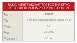
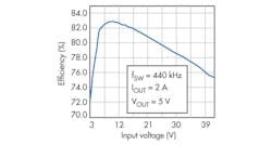
For higher efficiency, in this reference design the MAX16990 is used at a 440-kHz switching frequency (see the table).
Suppose an efficiency (Eff) of 85% and calculate the input current range that is equivalent to the primary inductor current range:


The secondary inductor average current range coincides with the output current range:
ILs(AVGMIN) = IOUTMIN = 1.8 A (23)
ILs(AVGMAX) = IOUTMAX = 2.2 A (24)
Now calculate the duty-cycle range. To do this, choose the external nMOS. To determine the nMOS ratings requirement, calculate the peak drain current that corresponds to the peak inductor current. Assuming a maximum LIR of 0.5 when the input and output currents are at their maximum, then:

Based on this information, a Fairchild FDS5670 nMOS rated for a drain current of 10 A was chosen for Q. The typical RDS(ON) of this transistor is 15 mΩ with a VGS = 5 V (i.e., the gate-source voltage provided by the MAX16990). The rated drain-source voltage for this component is 60 V, higher than the maximum drain-source voltage calculated by:
VnMOSDSMAX = VINMAX + VD + VOUT = 47.5 V (26)
Assume that the forward voltage of the rectifier diode (a Diodes Incorporated B350-13-F) is equal to 0.5 V. The maximum reverse voltage for this component is 50 V, higher than the maximum reverse voltage required in this application:
VDREVMAX = VINMAX + VOUT = 47 V (27)
Once we have this information, we can calculate the duty-cycle range and ignore RSENSE for now:


This duty-cycle range is compatible with the MAX16990. To guarantee continuous-conduction mode:


Based on this information, a Würth Elektronik 22-μH inductor 7443551221 was selected for Lp (IR = 6 A, ISAT = 6.5 A), and a Würth Elektronik 4.7-μH inductor 744311470 was selected for Ls (IR = 15 A, ISAT = 19 A). Using these inductors, when the input voltage is at its minimum and the output current at its maximum, therefore:


This results in inductors and nMOS peak current of:


InMOSPEAK = ILpPEAK + ILsPEAK = 7.071 A (36)
The nMOS drain-current rating and the inductors’ current rating comply with the values given by Equations 34, 35, and 36. Now calculate the series capacitor with the following formula, and then choose a commercial value higher than that:

The ESR of the series capacitor must be lower than the one calculated with:

The voltage rate has to be higher than 42 V, and the capacitor current rate has to be higher than:

So, a TDK C5750Y5V1H226ZT 22-µF ceramic capacitor was selected. Now it is possible to calculate the sense resistor:

A 15-mΩ resistor was chosen for RSENSE. In accordance with the design specification on the output voltage ripple, the constraints on COUT are:


Consequently, two Murata 47-µF GRM32ER61C476K ceramic capacitors with an ESR of 5 mΩ at the switching frequency 440 kHz were chosen. Using the electronic calculator, it is now possible to extrapolate the following component values for compensation so we can obtain a crossover frequency of 3 kHz with a phase margin of 60 degrees:
RSLOPE = 2 kΩ (43)
CCOMP = 33 nF (44)
RCOMP = 3 kΩ (45)
Figure 4 shows a schematic of this reference design and the selected external components.
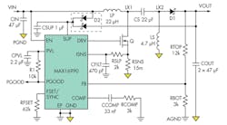
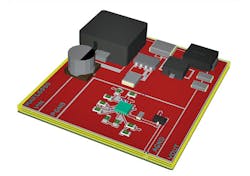
Figure 5 shows the design in a three-dimensional view.

Lab Test Results
Figure 6 shows the efficiency of the SEPIC regulator at full load versus input voltage (VIN).
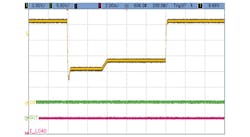
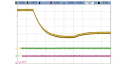
Figures 7 and 8 show the SEPIC regulator’s behavior during an automotive cold-crank event, where the battery voltage goes down to 3 V. In this reference design, the dual-diode D2 is used to supply the input voltage to the MAX16990 from the converter’s output when the battery voltage falls below the minimum input voltage of the controller IC.
Conclusion
We learned how best to select the external components and compensation to optimize the performance of an automotive SEPIC dc-dc regulator. Using the MAX16990/MAX16922 as example SEPIC converters, we demonstrated a SEPIC dc-dc regulator reference design for automotive applications. Test data illustrate the excellent performance of the reference design.
Andrea Longobardi is no longer with Maxim Integrated. He joined the company as a product definer and corporate applications engineer in 2011. He has a master’s degree in electronic engineering from the University of Pisa and specialized in automotive applications and IC design.
Cristian Cerutti is a principal member of the technical staff at Maxim Integrated with 12 years of experience in the microelectronics industry as an IC designer. He received his master’s degree in electronic engineering from the University of Pavia in Italy and joined Maxim Integrated in 2001, where he designed several ICs for audio and power conversion.
About the Author
Andrea Longobardi
Andrea Longobardi is no longer with Maxim Integrated. He joined the company as a product definer and corporate applications engineer in 2011. He has a master’s degree in electronic engineering from the University of Pisa and specialized in automotive applications and IC design.
Cristian Cerutti
Principal Member of the Technical Staff
Cristian Cerutti is a principal member of the technical staff at Maxim Integrated with 12 years of experience in the microelectronics industry as an IC designer. He received his master’s degree in electronic engineering from the University of Pavia in Italy and joined Maxim Integrated in 2001, where he designed several ICs for audio and power conversion.
Comment About the Article
To join the conversation, and become an exclusive member of Electronic Design, create an account today!

Leaders relevant to this article: