Download this article in .PDF format
Server-card designers have some tough choices to make (build or buy?) regarding the modules that power sections of their systems. While expertise on switching power-supply design continues to spread, the challenge of delivering very high currents to concentrated sections of a circuit board―what experts call increasing “power density”―may point to the use of pre-assembled and tested point-of-load (POL) supplies.
The telecomm “1/4 bricks” that deliver 30 A to the memory or I/O sections of a communications server card integrate control logic, pulse-width modulators (PWMs), power MOSFET transistors―even capacitors and possibly inductors. But a quarter brick would take up 3.33 square inches (2.28 × 1.45). Who can afford the board space?
Tradeoffs
Coming up with a smaller footprint generally requires some compromises as to what’s in the package and/or a lower power rating. The “tiny buck” package offered by many discrete transistor makers includes discrete power MOSFETs with the PWM in a small 5.5- × 5.0- × 1.1-mm package. The output current is about 6 A.
Some switch-mode design talent is required to put the buck regulator to use: While the package includes the semiconductors, the inductors and capacitors are not included. Additional printed-circuit-board (PCB) space would be required to route these components. The switching frequency of the buck regulators runs from 200 to 600 kHz, with a 95% peak efficiency.
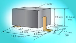
The 25 A required to power (say) the FPGA-based I/O sections of a computer card would need separate power transistors in the same package. One popular module offers 20 A from a 15- × 15- × 4.9-mm package—far smaller than a “1/4 brick” (57.9 × 36.8 × 12.7 mm)—but still quite demanding. (For reference, the diameter of a U.S. dime is 17.9 mm) The module includes capacitors in the package, and inductors can be integrated, relieving the board designer of a lot of decision-making.The semiconductor footprint can be further reduced, not just by putting the power output transistors in the same package with the PWM, but also by implanting them on the same chip. This makes use of a BCD (bipolar, CMOS, DMOS) process (also called biCMOS by some manufacturers) that implants power MOSFETs on the same substrate with CMOS control logic. The state of the art for BCD current delivery is about 10 A. The BCD process uses a horizontal conduction path for the MOSFETs, which makes the die size unruly for high currents.
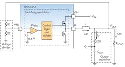
Texas Instruments sets a good example of a small footprint with its 30-A TPS53355 module. Each side of its QFN package measures 5 mm, and the height (considering an inductor could sit on top of the semiconductors inside the package) is only 1.5 mm. The switching speed is adjustable up to 1.5 MHz, and the rated efficiency is 96%. Adding an outboard PMBus controller would make this part a favored POL in new-generation server cards.
What You Need to Know About Voltage-Regulator Design
The legacy linear regulators based on a series-pass architecture remain popular: Widely multi-sourced, they are cheap (pennies apiece) and easy to use. A popular configuration offers only three pins for system builders to worry about: voltage input, voltage output, and a ground. But they’re notoriously inefficient, dissipating many watts of heat (especially a big gap exists between input and output voltages). This raises cooling costs in computer equipment and drains battery life in consumer electronics gear.
POLs using a switching-regulator topology, in contrast, are quite a bit more energy-efficient. They’re widely used in applications where cooling costs can run amok (like data-center server farms), and where the application provides little space for heat sinks (like flat-panel televisions). The downside of using switching power supplies—open-frame switchers, potted modules, or semiconductor dc-dc converters—is that they’re far more costly than three-terminal linear regulators, and they do require some engineering expertise to get them to work properly.
The typical switching power supply includes a PWM (with control logic), two or more power output transistors, and an LC network (using an inductor and capacitor). In operation, a saw-tooth oscillator in the PWM induces a stream of on-off pulses from the output transistors. The LC network essentially performs a filter function, charging up on a positive pulse and then discharging, effectively filling in the gaps between the pulses. The dc voltage level is determined by the frequency of the pulses and their “duty cycle”—the ratio between the transistors’ on-time and off-time.
In practice, if you want to raise the voltage level, you increase the switching frequency (e.g., pump out more pulses for a given time interval), though this will have a tendency to shorten the pulse’s duration. The values of the LC components must be chosen carefully to match the wavelengths of the pulse stream.
There are actually a lot of variables to juggle:
• High current output
• High energy-transfer efficiency
• Small PCB footprint
Even novice designers will tell you that the control is in the switching frequency of the modulator. Increasing the switching frequency accelerates the charging process for your output inductor and capacitor. This allows for the use of a smaller output capacitor and inductor.
Faster than Dirt
We’ve used this analogy before: Visualize your switching power supply as a steam shovel, transferring a mountain of dirt from one location to another. Each shovelful will transfer several cubic meters of dirt. But the process is slow and cumbersome, and several cubic feet of dirt are lost with each deposit. Now, re-imagine the dirt transfer using a teaspoon… only… the cadence of the transfer is 250,000 or a million times a second. The transfer mechanism is much smaller, and, because it leaves less residue behind, is more efficient.
However, the ability to arbitrarily increase the switching frequency is not a given. Current power supplies operate in the 250- to 500-kHz range. There are several reasons why this is the case. One has to do with the characteristics of the output transistors. The behavior of MOSFET switches, their ability to turn on and off in response to the PWM, depends on their current loading. The higher the current they need to turn on or off, the more sluggish the switches will behave.
In addition, server CPUs that demand at least 100 A require special MOSFET drivers (called DrMOS). Without them, you can have ringing, voltage overshoots, and droops under load. Elevating the switching frequency can make the sawtooth oscillator unstable. Power-supply designers will need to provide undervoltage lockout mechanisms as well as those for overvoltage conditions.
One workaround is to carefully match the performance of the output transistors with the regulator’s switching behavior. This isn’t particularly easy: The MOSFETs used in computer power supplies are generally optimized for minimal on-resistance (expressed in milliohms). That means they generate less heat in the ON state. However, it also increases gate capacitance, and makes the transistors harder to drive.
Furthermore, a mismatch exists between “high-side” and “low-side” MOSFETs in a totem-pole configuration (where one transistor’s drain is connected to the other transistor’s source). The drain of the high-side transistor is connected to the dc power rail; the source of the low-side driver will be connected to the common ground. The transistors need to be biased in a way that prevents the output voltage from latching to the positive rail, or crashing into ground. (Many designers look forward to the wide availability of gallium-nitride transistors, whose fast switching speeds would enable easier matching between power output switches and PWM controllers.)
Close in, the best hope for shrinking power is to increase the switching speed that will make enable a massive shrinking of the passive components (the capacitor and potentially the inductor). Large digital IC makers are becoming increasingly intrigued by the power-management function. If we can get dramatic results by just increasing the commutation speed of a switch-mode supply from 500 kHz to 1 MHz, what happens when your parallel switchers are operating at 10 MHz? Or 40 MHz, for that matter?
Manufacturers may see this as a way of building dc-dc converters in fine-line CMOS (90 nm and below) and integrating the voltage regulator on-chip with the system CPU. In the interim, we look to clever packaging for power-module components.
Looking for parts? Go to SourceESB.


