IGBTs are the device of choice for high power electrical power conversion systems. These are expensive systems that put great stress on power semiconductors. Reliability is a key factor in the design of such a system. We will examine several measures of the ruggedness of an IGBT to better understand the failure modes under various types of stress. By understanding these issues, the designer will be better able to design a power system that has a very high level of reliability.
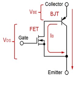
Several measurements can be used to quantify the ruggedness of an IGBT. The gate voltage rating is a safety measure, beyond which damage to the gate oxide can occur. The short circuit rating and the UIS ratings define the ability of the transistor to safely dissipate the power due to a transient surge. Each of these measures covers a different area of operation. Combined they offer insight into the survival of the IGBT during an abnormal transient event as well as provide operating limits to assure high reliability of the device. The equivalent schematic of an IGBT is shown in Figure 1.
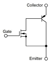
Table of Contents
The gate of an IGBT is a very high impedance connection that is used to control the conductivity of the device. The gate oxide is the insulation barrier that allows the electric field between the gate and emitter terminals to allow or not to allow, current to flow through the channel of the MOSFET.
Ideally, the gate drive pulse should be a square wave with no overshoot; however, this is rarely the case. Electrical transients from current and voltage transitions coupled with the parasitic inductances and capacitances of the system typically can be seen on the gate terminal.
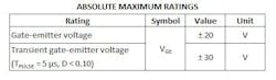
The gate-emitter voltage rating specifies safe levels of drive voltage that can be applied to the IGBT. Some data sheets specify only the DC limit of the gate voltage, while others include limits for the amplitude and duration of transient gate pulses.
The voltage across the dielectric, between the gate and emitter is an important parameter since high levels can cause tunneling of carriers through the dielectric. If the voltage exceeds the leakage limit, small imperfections called traps can cause a path for current to flow. This is called tunneling. Tunneling creates heat, which if allowed to continue for a sufficient period of time, can cause damage to the oxide, which in turn creates more traps. This process can quickly increase to the point where the gate oxide experiences significant damage.
It should be apparent that at higher gate voltages it is necessary to limit the duration of the event. This will assure that the temperature rise due to the tunneling electrons does not exceed a safe level. If the oxide becomes hot enough to cause damage, that damage will be cumulative. This is why both the time and duty ratio of the transient event are included on the data sheet.
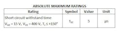
The gate voltage rating(s) can be found in the Absolute Maximum Ratings table located on the first page of the IGBT data sheet (see Table 1).
When checking out a new design, it is important to observe the gate-emitter voltage waveform, preferably with a differential voltage probe, to assure that the drive levels are within the specified limits.
The short circuit rating is a measure of the energy that the IGBT can withstand under a short circuit condition. In this condition, the IGBT is forced on, with a high voltage applied across the collector-emitter terminals. This causes a very high current to flow and very high power levels to be dissipated by the device.
In this condition, the IGBT is conducting, so all of its cells are enhanced and the current density is uniform across the active surface of the IGBT die. Therefore, heat is generated in a uniform manner across the die.
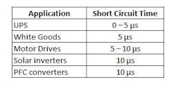
Some industries have standard requirements for this parameter, while others do not require a short circuit rating. Table 2 gives some standard short circuit requirements for various applications.
The short circuit rating is tested by applying a fixed voltage across the collector-to-emitter terminals and then biasing the gate on. This is tested while the IGBT is mounted on a heat sink and stabilized at a high temperature. For example, to evaluate a 600 V IGBT, you typically apply 300 to 400 V from the collector-to-emitter terminals and then bias the gate at 15 V. This is equivalent to a short circuit condition in a power converter. The short circuit rating is the amount of time that the device can withstand the enormous power being delivered to it before it fails.
The failure mode for this test is the heating of the die to the point where it no longer functions as a semiconductor. It is a fairly simple thermodynamics problem. Power is pumped into the die and its temperature increases based on the thermal mass of the die to the failure point.
To change the short circuit time, only one variable can typically be adjusted. The die size is fixed, the test conditions are normally fixed (gate voltage, collector-emitter voltage and heat sink temperature), so the current through the IGBT is the only available parameter that can be modified.
Figure 2 shows the current flow through the IGBT. The bipolar transistor is the main current carrying device and the FET provides its base drive. The current through the bipolar transistor under a given set of conditions is determined in part by its base drive. By adjusting the transconductance of the FET, the base drive of the BJT can therefore be controlled, and this is exactly how the short circuit rating is controlled. For a long short circuit rating, the transconductance of the FET is reduced so that its drain current is lower for a given drain-to-source voltage and gate voltage. This results in lower base drive current, lower collector current and thus a lower power level in the IGBT.
There is an engineering tradeoff here. A longer short circuit rating means a more robust IGBT, but the lower transconductance in the FET equates to a higher Rds(on) which directly affects the VCE(sat) of the IGBT, so conduction losses are traded for short circuit ratings. Short circuit ratings are shown in Table 3.
UIS ratings can give useful insight into the ruggedness of an IGBT; however, such information is not normally included on the data sheet. The UIS rating for an IGBT is measured just as it is for a MOSFET, storing energy in an inductor and then avalanching the IGBT, which then must dissipate that energy. This may appear to be a redundant test to the short circuit test; however, there is a significant difference between the two. In the short circuit test, the device is turned on and the current density is uniform across the surface of the die. For the UIS test, the device is biased off and must avalanche in order to conduct the current. This results in most of the current flowing around the perimeter of the IGBT, or in other words, there is significant current crowding around the edge of the device. Due to this difference, the amount of energy that can safely be absorbed under UIS conditions is considerably less than in the short circuit condition.
For example, ON Semiconductor’s NGTB40N120FLWG is a 40-A, 1200-V IGBT. It has been tested for UIS and has a capacity of 1.32 Joules. Its short circuit energy level is 5.13 Joules, calculated from the test data. This part is rated at 10 µs, but during testing the part survived an 11 µs short at a current of 819 A while supporting a voltage of 569 V, which results in the 5.13 Joule energy level. This is a ratio of 3.9 : 1 of short circuit energy to UIS energy.
While the UIS capacity of the IGBT will always be less than the short circuit capacity, this will not always be true for the packaged device. Many IGBTs are co-packaged with an anti-parallel diode. The breakdown voltage of the diode and the IGBT will never be exactly equal. If the diode breakdown voltage is lower than that of the IGBT, it will dissipate most or all of the energy in the UIS test, while the IGBT will always dissipate all of the energy in the short circuit test. The anti-parallel diodes are typically smaller dice than the IGBT and have a lower UIS rating--in some cases significantly lower. Therefore, UIS test results can vary greatly for similar rated devices depending on which die breaks down first.
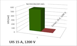
An extreme example of this can be seen in Figure 3. Both parts are designed for the same application and have the same voltage and current ratings; however, in the ON Semiconductor part, the diode has a higher breakdown voltage than the IGBT and thus has a very high UIS rating. The competing device has a very small diode which breaks down first and has a very low UIS rating.
An example of the value of this rating would be when the devices are used in a quasi-resonant, flyback converter for an inductive heating cook pad. In this circuit the line voltage is rectified with no filtering other than a small EMI filter. The flyback transistor is connected through a resonant LC circuit to the line and generates the magnetic field required to cause the pan to heat. If a line transient occurs in the building where the cooker is being operated, it will be imposed directly on the IGBT.
In the case of the ON Semiconductor IGBT, there is a high probability that the part will survive a transient. The other device will most likely not be so fortunate.
The circuit in Figure 4 is used to test the UIS of a transistor. Figure 5 shows the UIS test waveforms. The IGBT is turned on until the collector current reaches a predetermined level and then quickly turned off. The voltage on the inductor increases until it reaches the avalanche level of the IGBT or diode. At that time the energy is transferred from the inductor to the semiconductor. Once this event is complete, the package IGBT is tested and if it is functioning properly, the test is repeated at an incrementally higher current until it fails. The highest energy level before failure is the UIS rating of the device.
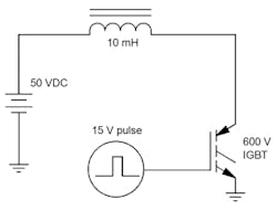
Figure 4. This circuit is used to test the UIS of a transistor.
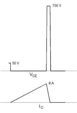
Figure 5. These are the UIS test waveforms for the circuit in Figure 4.
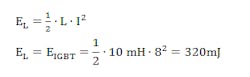
In this example, a 600 volt rated IGBT is connected to a 50-V DC supply through a 10 mH inductor. The current is ramped to 8 A and then the IGBT is turned off. The avalanche voltage for this part is 750 V. The energy dissipated in the IGBT is that of the inductor, which can be calculated by the equation
At this point, the device would be allowed to cool, and then would be retested at a higher current level.
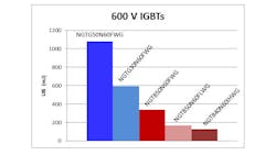
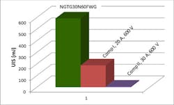
UIS ratings for several 600-V IGBTs produced by ON Semiconductor are shown in Figure 6. All of these devices can dissipate considerable amounts of energy in an avalanche condition. Figure 7 shows the UIS results for several 20- and 30-A, 600-V IGBTs. Again, there is a large difference in the UIS ratings for these devices.
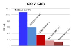
Figure 6. This chart shows the UIS ratings for ON Semiconductor 600-V IGBTs.
The gate voltage rating of the IGBT gives the maximum DC rating that the gate oxide can safely withstand. In some cases a transient rating is included. These ratings should not be exceeded or the reliability of the device can be compromised.
The UIS and short circuit ratings both test the ability of the die to absorb energy under unusual transient conditions. The short circuit rating is a good indicator of the ruggedness of the IGBT when the device is turned on and is normally specified in units of time and not energy. The UIS rating is a good indicator of the ruggedness when the device breaks down in avalanche mode. The short circuit rating is listed in the Absolute Maximum Ratings table, while the UIS rating is not normally given for an IGBT.
As with any electronic component, the design of the circuit that uses that component should assure that the part is always used at safe stress levels for maximum reliability.

About the Author
Comment About the Article
To join the conversation, and become an exclusive member of Electronic Design, create an account today!

Leaders relevant to this article: